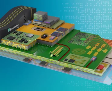
Pixel detectors made by Fraunhofer IZM are used in one of the largest and best known scientific centers worldwide. Since the discovery of the Higgs Boson in 2012, the researchers at CERN have been pursuing other groundbreaking discoveries.
Thomas Fritzsch explains to RealIZM just why micro-integration is needed in a machine measuring more than 26 kilometers in circumference – with the help of tram trains and onions.
Can you walk us through the most important parts of your work?
Thomas Fritzsch: Put simply, pixel detectors are sensors that detect particles. They are used in detectors for high-energy physics, for X-rays and for infrared radiation. They consist of an electronic ASIC, a CMOS chip that processes the signals, and a sensor – usually silicon – that generates the signals from charged particles, X-ray photons and infrared photons.
Are pixel detectors also used in other areas?
Thomas Fritzsch: Basically, they belong to the greater group of imaging detectors. Even the cameras in mobile phones do essentially the same thing. The difference from the pixel detectors we build is that the particles they detect have much higher energy. Conventional mobile phone cameras would fail because they are not sensitive enough for these particles. In order to detect these particles reliably, you need so-called hybrid detectors and a substrate specially adapted to the particles.
How do they differ from strip detectors, and what are they used for?
Thomas Fritzsch: Strip detectors are simply older, and the difference is one of design. They have the advantage that they are arranged on the top and bottom conductor tracks on the sensor, which
Does CERN use both technologies?
Thomas Fritzsch: Not really. The detector is located in a huge cavern, sunk underground and built in layers like an onion. The individual layers of the onion are the individual detector layers. We have a large magnet around it and this detector. There is a beam tube in the middle, where the accelerated particles from the big ring circulate, and there are crossing points in the area of the detector. That is where the particles collide – this is what you want to prove.
This means that if electrically charged particles are formed during the collision, they move on a spiral path in the magnetic field. The particles are so high in energy that they are not absorbed in the individual detector layers, but pass through all the layers like a needle. Based on the individual points obtained from the particles in the layers, it is possible to reconstruct the trajectory of the particles and deduce which particles had which charge and which velocity.
At Fraunhofer IZM, we are manufacturing modules for the core area, the inner tracking detector.
So it is not about the complete solution?
Thomas Fritzsch:No, but that is not demanded anyway. We are working very closely with the institutes of the CERN Consortium, for example the University of Bonn, directly with CERN, and with other internationally distributed research institutions. The whole detector is divided between different countries, as are the various tasks. One is responsible for the sensor development, one for the chip development, one for the contacting, one for the full detector assembly etc.
What exactly is the role of Fraunhofer IZM?
We manufacture the core components for the inner pixel tracking detector. These are the silicon hybrid modules. Hybrid means they consist of two parts: the read-out chip and the sensor.
We are speaking about a pixel array of diodes and the readout chips that read the signals. Each readout cell is connected to a pixel cell on a sensor. When a particle passes through the detector, a signal is generated in one of the pixel cells on the sensor and passed through the bump to the readout electronics. This signal is then processed further and sent to the actual data processing system via electrical and optical signals. At Fraunhofer IZM, we build the detection or sensitive elements with our assembly and interconnection technology. For this specific purpose, we are using fine-pitch bumping technology.
There are so many different technologies – why did you choose this specific one?
Thomas Fritzsch: Because this is the technology of choice to get high pixel density. And it is the only technology capable of connecting a pure pixel matrix directly to an underlying chip. It involves distances of 50
What is the current status, and what is the target?
Thomas Fritzsch: There are two different directions for us in the house: the tracking detectors for colliders for the so-called high-energy physics, which mainly takes place at CERN.
This is now the next phase for the next upgrade of the detectors. At the moment, the collider is switched off for two years. An upgrade is currently underway, and the ATLAS and CMS detectors are to be renewed starting from 2024. The goal at CERN is not to increase the size of the ring where the particles move, but to increase the density of particle packing.
That’s a good comparison to the tram system: One would like to have more trains (particle bunches) on the ring, so that there are more stations (detectors) at shorter intervals. The readout chips have to read the signals faster, so that the data processing is already completed before the next particles arrive. And they must become more radiation-resistant, because more charged particles are formed during the collisions. These are the requirements for the next upgrade. This is called “high luminosity” because the luminosity is increased, i.e. the number of particle packages in the ring and the interval between collisions.
What would these new improvements enable us to do?
Thomas Fritzsch:The great research success of the LHC was the discovery of the Higgs boson, which explained how particles get their mass. This was the missing link to explain which particles have mass and which do not, or how they are formed. Theoretically, it had been postulated long before that there must be a particle that gives other particles their mass through their interaction, while other particles float through space without mass.
Since the discovery of the Higgs boson, practically no new discoveries have been made. Therefore, with the upgrade, the new approach is to increase the collision probability. Another example: two cars colliding at 100 kph generate more energy than two cars colliding at 30 kph. One would like to generate higher energies for the collisions in order to generate higher energetic particles. The Higgs boson could not have been produced with a particle accelerator before the LHC, because it would not have the size needed to accelerate the particles to this speed and energy.
How can we improve our pixel detectors?
Thomas Fritzsch: The ATLAS detector we built in the first iteration consisted of approximately 1.5 square meters of silicon area. Now we are talking about 10 square meters of silicon. This means that we now have to think about how we can reliably implement the assembly and connection technology with higher throughput. The read-out chips used to be on 200 millimeter wafers and are now on 300 millimeter wafers. In addition to this, we are working on larger chips. At the end, they should be 2 x 2 cm², and there should be four instead of two chips on the modules. This will create large modules from which the detector can be assembled. We have to make sure that all bumps are placed on the chip, that they have the same height and that they are reliable in the bonding processes.
How does this improvement help us?
Thomas Fritzsch: For us, this is a further development to make this technology interesting for industrial partners as well. When we started hybrid module manufacturing in 2000, this small interconnection pitch was not yet state-of-the-art. But it is developing in various other application areas, e.g. medical imaging technology. X-ray devices are increasingly using hybrid
What are the biggest challenges you see in this area?
Thomas Fritzsch: Doing it all in the time we have. Especially at CERN for the upgrade phase, the time schedule is tight and the slot for the production of the modules must be correctly adjusted to the production of the wafers, up to the installation of the complete detector. Our work must run in sync with the work of our partners.
What projects are currently running?
Thomas Fritzsch: In the field of imaging detectors, we are cooperating with DESY in Hamburg, SLAC in Stanford in the United States, and with different research groups in the various consortia. Our task is the manufacturing of modules for X-ray laser cameras. In cooperation with researchers from all over the world, we are getting involved in various productions of detector modules.
What sets Fraunhofer apart from the competitors?
Thomas Fritzsch: At Fraunhofer IZM, we have the advantage that we have both main steps available in house: the bumping on wafer level and the flip chip assembly. So, we can offer the whole chain from wafer processing to bare module assembly.
With us, it is mostly about keeping the electronics as small as possible. The collider is huge: Is miniaturization even necessary?
Thomas Fritzsch: There we go again with the onion principle. The onion is very big, but we want to get to the information inside. A pixel is always a structure, from which one would like to pull out
This interview was conducted by Yulia Fedorovich and edited by Marieke Lienert from Fraunhofer IZM Marketing & Business Development department.

Add comment