Modern society is relying more and more on connected, digitalized, and automated technology – an epochal change that touches on all aspects of business life, including the manufacturing of products. Fraunhofer IZM is at the forefront of this trend, creating the technical solutions that make digital manufacturing possible.
Steve Voges, researcher at Fraunhofer IZM, tells RealIZM how to combine manufacturing, production environments, equipment, materials, security, and products under the one conceptual roof of “Industry 4.0”.
In a nutshell: What does industrial digitalization mean?
Steve Voges: Defined very broadly, industrial digitalization is about integrating management and manufacturing processes, materials, and other things relating to production, which are all interconnected and networked, in digital models, by which I mean the parameterization of all of these aspects in digital formats, based on domain knowledge and data. All the data we collect in product development is stored in databases for quick and easy access. That data is then analyzed by AI, e.g. with machine learning, and used to make predictions.
In this case, we often talk about digital twins. Humans have bones, organs, certain patterns of behavior, memories and so on, which are all linked together and define us as human beings. It’s the same thinking behind digital twins – all components of production are connected, and they can exchange data and interact intelligently with each other. In addition, they know their states at different points in time.
Industry 4.0 currently collects and analyzes data mainly from the manufacturing phase and through the product’s life. The next step up in evolution would be the digital twin, where materials and processes are modelled to allow us to predict and evaluate how changes to one parameter can affect the entire system.
How can companies benefit from industrial digitalization?
Steve Voges: If you have modeled your materials and processes, then you can design, simulate, and optimize a digital prototype. You then use this optimized prototype to go into manufacturing. A digital model of the development project can help reduce the time and financial assets that you need to invest.
What does digitization mean for Fraunhofer IZM?
Steve Voges: At Fraunhofer IZM, we are trying to describe the processes (flowcharts, Ishikawa diagrams) in an abstract way and to collect as much and as diverse manufacturing data as possible to optimize processes based on our knowledge and with AI support. On top of that, we are promoting digitization by developing datasets and material laws to help us evaluate changes in properties, like what happens in thermal ageing (see our “Mature” project with our partner institute IFAM) or how moisture is accumulated or retained in a material. We use these insights for e.g. more reliable service life predictions. In other words, we are developing concepts for the digital twins of materials and manufacturing processes in microelectronics.
What equipment are you using for your digitalization work at Fraunhofer IZM?
Steve Voges: Speaking generally, we are not using any specific tools for digitization, other than databases or the ever present Excel spreadsheet. Typically, we would be working with production machines like those that you can find in real factories. For example, we have a fully equipped assembly line for clean-environment manufacturing (close to ISO 6 to 7 standards), operated by trained staff. For manufacturing quality, we are shooting for IPC 610 standards. We have also material application systems, such as precision material dosing for a wide spectrum of materials, a dedicated silicone lab with dispenser/jetter, printer and 2K potting equipment for HF module manufacturing, as well as analytical tools for process characterization. On top of that, we have various molding systems, like transfer molding or compression molding on 200 mm & 300 mm wafer sizes or large-area panels, up to 610×457 mm², as well as a dedicated sensor mold tool to help us determine process-related material properties. This equipment gives us the data that we have to collect for further analysis.
Moreover, we are using a Manufacturing Execution Systems (MES) to model, manage, and plan production runs, and the PMS and the WMS – process management and warehouse management systems – for tracking processes and digitalizing warehousing.
All this gives us data that can be used for our work on digitization.
Are there any examples of what you have achieved with your research?
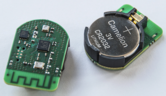
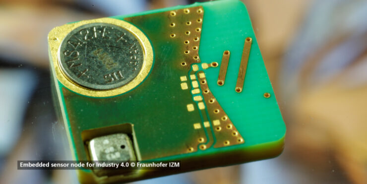
Steve Voges: One example is the PCB 4.0 project. For this project, we developed a sensor node that is extremely miniaturized to get it integrated into its mother PCB by means of substrate embedding. It can collect data, like temperature, pressure, vibration, or humidity, during the production of the actual mother PCB. A larger version, depicted below, can be used to monitor environmental data or process-specific data, such as as vibration / acceleration, inside the production equipment itself, that is, outside of the actual PCB.

On another current research project SiEvEI 4.0, we are taking this to the next level:
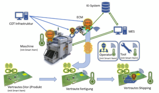
First, we want verifiability and correct authorization in the manufacturing of electronics, especially for sensitive assemblies, e.g. for power plants, aviation, spaceflight. All this has to be tamperproof and traceable to guarantee the safety of the product. In trusted manufacturing, an edge computing module (ECM) containing a certificate is linked to each machine. The ECM in this case is also a gateway between the smart workpieces and the central AI/cloud. The smart workpieces also contain a certificate store as a part of a smart secure item (SSI). The SSI is based on the PCB 4.0 sensor nodes and can store the so-called Chain of Trust (CoT), which is a chain of tamperproof manufacturing data where each link corresponds to a step in the manufacturing of the workpiece. The individual chain links are also given appropriate certificates to verify that the machine, operator, material etc. is actually authorized for that step in the manufacturing process. Optionally, sensitive information can be encrypted, so that only authorized persons can read the information. Thanks to the CoT, we know by whom, when, how, and where the individual process steps were carried out, and this data can be reliably tracked without being at risk of manipulation.

For our second goal for SiEvEI 4.0, we are also trying to record and monitor not only workpiece data, but also process data, machine data (e.g. movement patterns, forces, and temperatures) as well as environmental data (e.g. room temperature and humidity) with the sensor network. The digital data is collected, aggregated, mapped, and, if need be, pre-processed by an edge computing module, so that only relevant data is sent to the central AI in the cloud. This data is then analyzed by the central AI, using a range of AI methods, to predict how individual process steps could be optimized in terms of yield or performance. As a result of this analysis, the system can feed back recommendations for certain tweaks to parameters to improve the production process.
We are currently testing this procedure for the process of applying solder balls to modules.
What are the challenges in this project?
Steve Voges:The first challenge is how we get the data from the machine manufacturers’ platforms. The difficulty is that many machine manufacturers have either proprietary interfaces or one of the many standardized (e.g. OPC UA, IPC CFX) software interfaces. So far, there is no industry-wide agreement on a standard. Until we have that, we have to keep finding a custom software solution for each machine manufacturer.
The next challenge is how to describe processes and materials as generically as possible. The keyword here would be process ontology. Related to this is the problem of data mapping. How do we homogenize disparate data sources, such as machine interfaces, user input, and other software systems in a common understanding of the data model, so that the AI system can then analyze this data holistically?
Are you already planning a follow-up project in this area?
Steve Voges: Yes, we are discussing it at the moment. We would like to work on the idea of connecting digital twins of materials with digital twins of processes along the process chain to better understand the interaction between material properties and process parameters. The overall goal is to model complex process chains to optimize yield, reliability, and costs. But these are no low-hanging fruits – we’ll be working on this for the next ten years at the minimum.
Another follow-up idea is to collect the important image data as well. Since the file sizes are large in that case, you need an extra-small, but powerful module attached directly to the machine, which would pre-process the image data using AI methods and forward only the relevant bits and pieces.
Do you already have an idea for how this technology could be commercialized?
Steve Voges: We are the people with the domain knowledge you need for electronics manufacturing, and we are developing the knowhow to model single processes and process chains in a way that should adapt easily for our customers’ digitization infrastructure. Long story short: We can help digitize your processes, fast. Helping our customers kick-start their Industry 4.0 implementation with the best support they can get: That is the vision that I have.
ACKNOWLEDEMENTS
For excellent research, excellent partners are paramount – we are working with Siemens AG, Sensorik-Bayern GmbH, Wagenbrett GmbH & Co. Kg, WIBU-SYSTEMS AG, the Technical University of Berlin, the University of Bielefeld, and ASM Assembly Systems GmbH & Co. KG.


Add comment