The new generations of semiconductors with a wider band gap (WBG), such as silicon carbide (SiC), have the potential to put electric mobility in the fast lane. This is because they yield significantly higher efficiency compared to conventional silicon IGBT circuits and offer numerous other advantages, such as better temperature stability and less power loss.
In his interview with RealIZM, Lars Böttcher, head of the “Embedding and Substrate Technologies” working group at Fraunhofer IZM, spoke about the challenges of packaging SiC power semiconductors for the electric vehicle industry.
Starting with the basics: What are the advantages of SiC power semiconductors for electric vehicles, and where are they mainly used?
Lars Böttcher: To date, SiC power semiconductors have primarily been used in traction converters and inverters for electric vehicles. First, you want to convert the DC current from the high-voltage battery into AC power for the electric engines. Second, you need a way to convert the AC current that electric vehicles get from their chargers into direct current for the HV batteries. SiC power semiconductors do not yet play a major role in the battery management systems of electric vehicles. For cost reasons, silicon technology is still used there.
SiC power MOSFETs are a very good option for the highly efficient drive converters with high power density you get with electric vehicles. Put simply: they are efficient, reliable, and compact. Compared to silicon IGBT circuits, silicon carbide (SiC) gives you significantly higher efficiency. SiC is more reliable in terms of temperature stability, allows higher operating temperatures, and has higher dielectric strength.
Optimizing efficiency is not only important for faster switching, but also for improved range and for a longer service life of the batteries in electric vehicles. Another decisive advantage is the lower power loss, which makes it possible to significantly reduce power densities. In the engine compartment of a vehicle, every cubic centimeter is worth its weight in gold. The ability to minimize volume and weight via the traction converters and control inverters gives you a competitive advantage.
But the high efficiency of SiC also poses exciting challenges for us technologists. The dielectric properties of SiC directly impact the development of gate drivers and protective devices, among other things. In addition to design challenges, we have to make sure that the drive converters are properly isolated from the sensitive low-voltage electronics of the vehicles.
Wherever power is converted, heat gets generated. Understanding and mastering the thermal design of SiC modules for the specific application is essential when you compare it to traditional IGBT modules. We have to match the materials – the electrical insulation and the thermal path – up with each other.
You can add to this the innovative nature of this technology. All materials surrounding the semiconductor must be resilient, and the individual components must withstand temperatures of up to 175°C over their entire life cycle.
What role does packaging technology play in the functionalization of SiC chips?
Lars Böttcher: To put it bluntly: I can’t just plug a piece of silicon carbide into a socket. Chips have to be functionalized using packaging and interconnection technologies. This can be done either with classic wire, ribbon or clip bonding technologies, or with innovative techniques like PCB-based embedding, SKiM or eMPack technology from Semikron Danfoss. The world of packaging and interconnection, in which our research institute has been operating successfully for over 30 years, is a key bridge between the wafer world – the fabs that produce the wafers equipped with semiconductors – and the actual applications. The fabs supply the semiconductors, which are at first of no use to Tier 1 suppliers or vehicle manufacturers without the corresponding packaging and interconnection. The packaging and interconnection is the basic prerequisite for creating individual packages from the devices and, in turn, build an inverter from the individual packages.
In my working group “Embedding and substrate technologies”, we focus on the technological approach. We have many years of experience with embedding Si, SiC, and GaN chips, and we have a complete state-of-the-art processing line. One of Fraunhofer IZM’s strengths lies in our interdisciplinary collaboration. We cooperate very closely with the “Power Electronics Systems” working group headed by Professor Eckart Hoene. This enables us to design SiC modules for our clients, from the electrical switching technology to the structure of the layers.
Our research institute has experts in material properties as well as teams that carry out load change tests and reliability assessments and investigations, such as the change from storage temperature to high temperature, according to customer-specific requirements. With each new generation of power electronics, we can get better functionality and lower costs. At the same time, this always brings greater challenges in terms of reliable insulation and thermal management. For new types of semiconductors with extremely high bandwidths, standard tests with rigid test methods will not (or no longer) be sufficient for evaluating the (remaining) service life; instead, custom “application profiles” are likely to dominate this area of activity.
Fraunhofer IZM has been involved in the development and implementation of embedding technologies for inverter structures in high-voltage traction inverters for automotive applications. We do this on behalf of our industrial customers and as part of several publicly funded projects like SiCModul, SiCefficient, and HiEFFICIENT. From the feasibility assessment for a new technology to the actual implementation of a traction inverter structure, we check the technological feasibility of customer-specific requirements in terms of thermal and electrical design. We are able to produce prototypes and a manageable number of samples and provide support for a rapid transfer to industrial production in Europe with our cooperation partners.
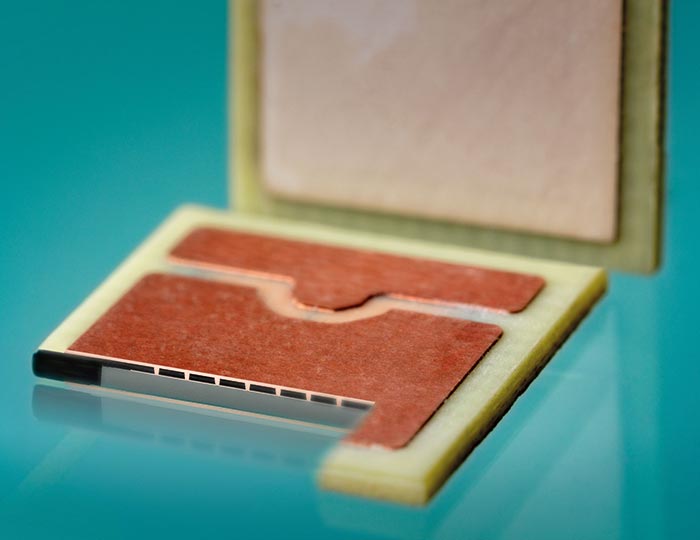
Left: Embedded silicon carbide on the way to series production for electric mobility applications, SiCModul project | © Fraunhofer IZM I Volker Mai
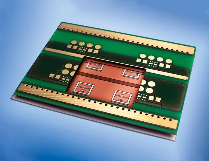
Right: A look into the power electronics (model) in a circuit board for 90A (HHK project) | © Fraunhofer IZM I Volker Mai
Why are innovative packaging processes needed for SiC semiconductors?
»The key to the success of SiC lies in the packaging of the semiconductors. Standard packaging processes are not enough to reap all of its benefits.«
Lars Böttcher, Group Manager »Embedding and Substrate Technologies«, Fraunhofer IZM
Traditional wire-bonded modules very quickly reach the limits of what is physically possible in terms of power density and electrical properties. Wire bonds only have a limited service life during active power cycles, as each component is actively energized and heated by 100 to 120 Kelvin in a very short time.
Compared to other connection technologies, wire bonds are also much more limited in their electrical properties. You cannot achieve the fast switching speeds and low losses with wire bonds, where relatively strong parasitic effects occur in terms of inductance due to the electrical connection to the semiconductor itself. This means that existing packaging processes must either be improved to suit SiC, or we need completely new processes.
The focus tends to be on the development of new methods. A reference example from current technical literature would be the eMPack power module platform for automotive applications made by Semikron Danfoss. This involves wiring via a flexible substrate, which is placed on both the front and back of the semiconductor using silver sintering.
Conventional packaging processes using wire bonds and frame modules on ceramic substrates are two-dimensional. It is not possible to integrate additional current-carrying layers directly above the semiconductors in order to apply additional components, which would favor lower-loss switching by reducing parasitic effects.
In our experience, PCB embedding technology is the best option for a three-dimensional design. We are also seeing increasing interest in this from Tier 1 and OEM partners. This process allows us to optimize electrical performance, thermal management and insulation reliability and to minimize parasitic effects and switching and conduction losses.
As technologists, we can make numerous adjustments. The two key aspects that speak in favor of PCB embedding technology are: the significant improvement in electrical switching behavior due to the low-inductance connection and the significant increase in reliability. It has been proven that direct copper metallization for silicon carbide power semiconductors leads to a significant increase in active load change cycles, which translates into a longer service life. As part of one project, for example, we eventually aborted a test series after more than a million load cycles. With wire bonds, significant failures usually occur after around 100,000 to 120,000 cycles.
The industry is showing increasing interest in embedded SiC power semiconductors for high-power electric drives, particularly traction inverters for hybrid and all-electric vehicles. There are many reasons for this. Embedded SiC modules do not differ fundamentally from wire-bonded SiC inverter modules in terms of switching capacity. The latter are used in vehicles. The difference lies in their efficiency. Embedded SiC modules offer improved electrical switching. The reduction in parasitic inductances reduces switching losses. In addition, the volume and height of the embedded modules and, by implication, their weight can be minimized. Saving just one or two SiC semiconductors per module means real cost advantages.
What are the advantages of pre-packaging SiC modules in terms of reducing losses or the risk of individual modules failing?
Lars Böttcher: Let’s take a fictitious example: A 3-phase inverter with three half bridges is equipped with over 20 SiC power semiconductors per half bridge. If just one of these SiC modules fails or is damaged, the entire half bridge would be unusable. Economically, this would be a major loss. In our opinion, SiC pre-packaging is recommended to significantly increase the yield, e.g. on a ceramic insulation. In the SiCeffizient and DauerPower research projects, we used this method to form inverter modules on a high-current PCB, implemented with a low-inductance connection.
During pre-packaging, the SiC modules are assembled analogously to a complete half-bridge, then embedded in the PCB material and wired to the outside with micro-via copper metallizations. The result is individual chips that are 100 percent robustly packaged and tested in the material, which can then be used on either SMDs or high-current PCBs. With the pre-packaging approach, the risk of losing over 20 other modules at the same time in the event of a single faulty SiC module is low. One disadvantage that should not go unmentioned is that pre-packaging limits what you can do in terms of a reduction in volume and the level of power density.
What further developments and research can be expected with regard to alternative semiconductor materials with a large band gap?
Lars Böttcher: On top of its electrical properties, SiC has the advantage that it is ideally suited for high-voltage applications in the automotive sector. For example, a 1200 V SiC MOSFET enables very efficient operation at battery voltages in the 850 V range. GaN semiconductors, on the other hand, are so far mainly used in the lower voltage range with very low voltages, for example in high-performance chargers for cell phones that switch up to 100 watts. Occasionally, GaN semiconductors are available for applications in the 850 volt range. However, the idea of 1,200 volts is still being developed. Should such semiconductors based on GaN be available in the future, they would be a good and inexpensive alternative to SiC. Research is also being carried out into alternative semiconductor materials with a large band gap, such as synthetic diamonds, gallium oxide (Ga2O3) and aluminum nitride (AlN). To our knowledge, no semiconductors ready for series production have yet been realized.
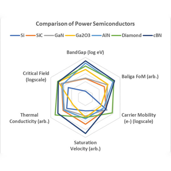
Comparing power semiconductors | © Fraunhofer IZM Internal Report
What is your forecast for the market for SiC semiconductors, and how has demand developed in recent years?
Lars Böttcher: SiC technology has become more mature. Nevertheless, the challenge is that the single crystals still have many flaws even under optimal growing conditions. Manufacturers are well on the way to increasing the yield per wafer and reducing production costs. The demand for SiC is actually higher than existing production capacities allow. Semiconductor manufacturers are therefore investing heavily into existing and new wafer production sites in order to be able to manufacture formats of at least 150 mm and 200 mm in diameter. Yole forecasts a market volume of around 1.5 billion US dollars for SiC in 2022, with the volume expected to quadruple over 6 billion US dollars in 2027.
Further information:
In our online expert series “Powering the Future – Innovative Technologies for Power Electronics Modules with SiC and GaN Semiconductors“, Fraunhofer IZM experts provide a real insight into the latest approaches and technologies, highlight application scenarios, and address the challenges and opportunities in the customized development of power electronic modules.
30.1.2024: Novel Concepts for fast switching power converters Prof. Eckart Hoene
13.2.2024: Wafer-level process technologies for SiC/GaN power electronics Dr. Piotr Mackowiak
27.2.2024: Highly reliable Interconnect Processes for Power Electronics Dr. Matthias Hutter
12.3.2024 Novel Integration Concepts for Power Electronics – PCB Embedding for Sic and GaN Semiconductors Lars Böttcher
26.3.2024 Reliability Challenges of Power Electronic Modules Dr. Stefan Wagner
Participation is free of charge, registration is required. Register here!