Sovereignty when it comes to sharing data: that would make the European semiconductor industry not only more resilient in its supply chains. It could also lay the foundations for more sustainable production processes. In this endeavor, Fraunhofer IZM has taken over the technical lead for sustainability in the research project »Semiconductor-X«.
The project includes work on a bottom-up data model and accompanying methodology for calculating the CO₂ footprint at the level of individual products (i.e. their Product Carbon Footprint, PCF), using the example of a single chip. The thinking is that this will offer more insights into current technical and regulatory frameworks from »Catena-X« in terms of how well they could be transferred and applied in the semiconductor industry. In close collaboration with other »Manufacturing-X« initiatives, this has the potential to advance harmonization and interoperability in PCF determinations across different sectors of industry, through the power of digital twins and special data ecosystems.
Dr. Chris Eckstein, head of the »Life Cycle Modeling« working group at Fraunhofer IZM, has met RealIZM to speak about how these approaches could help take product carbon accounting in the semiconductor industryto the next level. His vision: largely automated, consistent PCF calculations foreven complex semiconductor product supply chains.
The Carbon Footprint of the Chip Industry: Comparable CO2 data as a tool for decarbonization
With the »European Chips Act«, the European Union has set itself the goal of doubling its share of global semiconductor production to 20 percent by 2030. This is meant to strengthen Europe’s technological sovereignty. But it also impacts the industry’s emissions balance. Current projections indicate that greenhouse gas emissions associated with semiconductor manufacturing in Europe could increase by at least fourfold. Even with a significantly greater share of renewable energy, the resource-intensive production of semiconductor chips would become a major driver of emissions. In a scenario of consistent growth in production, European chip manufacturing could emit more greenhouse gases by 2030 than the European chemical industry did in the benchmark year 2021.¹
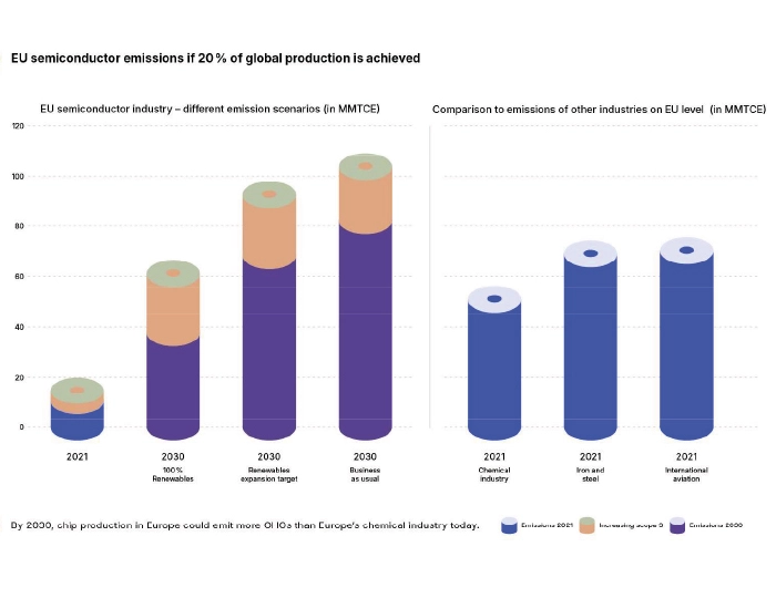
EU semiconductor industry emissions if the goal of 20% of global production is reached. | In: Julia Christina Hess: Chip Production’s Ecological Footprint: Mapping Climate and Environmental Impact. In: interface (2024), p. 48
Developing standardized methods for calculating the PCF is a key challenge when trying to identify and seize ways to decarbonize the industry’s value chain. Transparency about the methods for determining the PCF is crucial, as Dr. Chris Eckstein emphasizes: »The metrics must be based on clear and traceable calculations, so that any differences can be clearly attributed to the product and its manufacturing processes, and so that discrepancies in the calculations can be spotted.«
Standardized CO₂ Accounting for Semiconductor Products
»Our task is to evaluate the PCF calculation frameworks (Catena-X Product Carbon Footprint Rulebook) and check the semantic PCF data exchange models presented by ›Catena-X‹ to see if they are fit for purpose in the semiconductor industry, using concrete examples from the field. To this end, we came up with a method that takes the ›Catena-X‹ framework into account. This shows us how meaningfully it can be integrated in semiconductor manufacturing and its upstream supply chains. The data spaces developed in ›Semiconductor-X‹ are used to share data between the actors of the supply chain,« Chris Eckstein says about the project work. The proposed approaches could form the basis for robust life cycle assessments along the entire value chain. At the same time, they point a way forward to a more digitized and automated industry in which sustainability is systematically integrated and promoted with measurable effect.
A single chip is generally not a standalone product, but rather a component of complex electronic systems such as smartphones or vehicles. If such end products are to get Digital Product Passports (DPP) in the future, the necessary sustainability data must be made available throughout the supply chain.
»We have developed a methodology that enables us to calculate and compare the CO₂ footprint of semiconductors, thereby demonstrating how a Catena-X-compliant, granular, bottom-up PCF calculation can be implemented in practice.«
Chris Eckstein, Life Cycle Modeling, Fraunhofer IZM
»Semiconductor-X« comprises three areas of relevance: resilient value chains (Cluster 1), digital networks and semantic data models for optimizing factory and supply chains (Cluster 2), and sustainable semiconductor production with life cycle analyses (Cluster 3). Fraunhofer IZM is part of Cluster 3.
From Catena-X to Semiconductor-X: Standards as a Key to Success
Digital Data Ecosystems for a Resilient Industry
»Semiconductor-X« is part of the global collab project »Manufacturing-X,« which is pushing the development of a secure, cross-industry data ecosystem for the manufacturing sector. A collaborative data network was already established for the automotive industry’s value chain through the »Catena-X« project (duration: August 2021 – July 2024). For »Semiconductor-X,« this preliminary work is being adapted and key concepts are being applied to the domain-specific requirements of the European semiconductor industry.
A key focus is the systematic evaluation of the »Catena-X« framework regarding its applicability to the semiconductor industry and its compatibility with established methods for calculating the PCF. »The methodological framework of ›Catena-X‹ builds on the relevant ISO standards for life cycle assessments (ISO 14040/44/67) and makes them more specific and detailed,« Eckstein explains. He draws a positive conclusion: »In our view, the ›Catena-X‹ approach is fundamentally well-suited, as it consistently consolidates established requirements and creates a sound foundation for robust PCF calculations.«
What the »Product Carbon Footprint« Really Means
The »Product Carbon Footprint« (PCF) refers to the total of all greenhouse gas emissions, expressed in CO₂ equivalents, generated throughout the defined life cycle phases of a product. The scope depends on the defined system boundaries (e.g. based on the »cradle-to-gate« or »cradle-to-grave« principle).
The goal of the PCF is to quantify a product’s climate-related impacts, identify emission drivers along the value chain, and establish a comparable basis for reduction measures, reporting, and strategic decisions. The calculation is based on methodological guidelines for life cycle assessment (LCA), including clearly defined assumptions, allocation rules, and emission factors.
The calculation is based on methodological guidelines for life cycle assessment (LCA), including clearly defined assumptions, allocation rules, and emission factors.
Why a Chip Is Not a Simple Product
Manufacturing a single chip is a highly complex process involving several hundred steps. Front-end processes in wafer fabrication involve a few hundred to over a thousand steps, depending on the technology being manufactured. Added to this are back-end steps, such as assembly and bonding, as well as inspection and testing, each of which has product-specific energy, material, and process profiles.
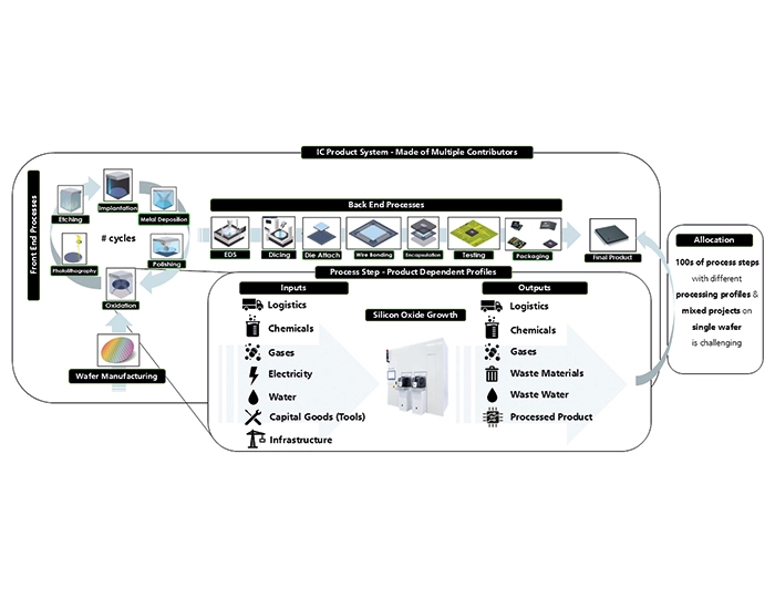
Complex process chains in semiconductor manufacturing: Hundreds of process steps and multiple chips per wafer make CO₂ allocation difficult. | © Fraunhofer IZM | Chris Eckstein
One of the fundamental challenges in calculating the carbon footprint of semiconductors is where to allocate the emissions. Given the enormous complexity of any semiconductor manufacturing facility, it is understandable that it is still common practice in the industry to follow a so-called top-down approach. Put simply, this takes total input and output flows and allocates them to the wafers or final chips produced. In modern manufacturing facilities, different products or design variants are also frequently produced in parallel on process lines that partially overlap, which makes it difficult to attribute energy and material consumption to any individual chips in a causally meaningful manner.
Semiconductor-X: A Granular Life Cycle Assessment Model for Semiconductor Manufacturing
The key outcome of the work done at Fraunhofer IZM as part of the »Semiconductor-X« project is a bottom-up data model and associated methodology for a sample chip. Data collection was carried out in close collaboration with the Fraunhofer Institute for Electronic Microsystems and Solid-State Technologies (EMFT), where real production and process data from applied microsystems technology were incorporated into the PCF modeling.
On this basis, the existing framework from »Catena-X« was transferred to semiconductor manufacturing (front-end and back-end) and refined for this unique domain. The PCF was defined as a »cradle-to-gate« assessment, so that all emissions from raw material extraction to the fully processed chip are taken into account.
A 200-mm wafer in the front-end and a package (QFN) in the back-end served as the declared units to establish a basis for comparison. This marks a methodologically consistent and practically tested bottom-up approach has been developed that meets both the requirements of industrial data repositories and the standards of life cycle analyses.
CO₂ Footprints as a Future Selection Criterion in Supply Chains
Given the high complexity of carbon footprint accounting in semiconductor manufacturing, Chris Eckstein believes that the sustainable transformation of the semiconductor industry can be accelerated through automated PCF calculation and communication based on uniform standards across the entire supply chain. This would allow companies to efficiently integrate emissions data into their product portfolios—which may include several thousand different product variants—and make informed decisions regarding decarbonization.
If companies provide their CO₂ data in a standard data ecosystem, inquiries regarding product carbon footprints could be answered in a similarly standard manner, and key metrics could be seamlessly incorporated into the overarching assessments.
Although CO₂ values do not yet play a direct role in customers’ purchasing decisions, Eckstein notes that this could change. In tenders in particular, the carbon footprint is becoming increasingly important as a quality and awarding criterion to promote sustainability in the supply chain. In any case, feedback from the partners involved in the »Semiconductor-X« consortium has already demonstrated that there is a real need within the industry for interoperable and standardized methods for determining emission values.

Calculation and sharing of the product carbon footprint along the supply chain. | © Fraunhofer IZM
Sustainability as a joint effort in the data room
In addition, Fraunhofer IZM assumed a coordinating role in the »Sustainability« project cluster. Through ongoing bilateral discussions with project partners along the supply chain, the »Catena-X« framework was publicized and industry-specific requirements for life cycle analyses were identified and categorized. These findings were incorporated into the development of the bottom-up data model and accompanying methodology, which systematically consolidates and expands key methodological guidelines.
In addition, Fraunhofer IZM continues to support several partners in developing their life cycle inventories (LCI (LCI) analysis) and process-specific use cases and supply chain demonstrators. In liaison with other »Manufacturing-X« initiatives, it also supports communication to ensure the interoperability of PCF determination across sectors.
Data Challenges and the Operationalization of Catena-X for Refining the PCF Methodology
Collecting the relevant data required to calculate a semiconductor PCF is an immense challenge. It is characterized by the technological complexity of manufacturing and the logistical intricacies of globally distributed production sites, coupled with a high degree of diversity in the products. This requires valid, consistent, and standardized data. To get this data, it needs a production environment in which all relevant mass and energy flows can be recorded on a process and product-specific basis, digitally documented, and subsequently aggregated along the entire value chain to be converted into CO2 equivalents together with logistics data. The development, implementation, and integration of a sensor infrastructure with digital interfaces in complex industrial facilities, as well as the creation of product-specific data models, involve considerable effort and costs. It is not surprising that top-down allocation is the current standard practice.
Equally important is the handling of sensitive production data. In the semiconductor industry in particular, detailed process data is a key factor in competition. At the same time, ensuring data sovereignty when sharing PCFs is a central prerequisite for any cross-organizational collaboration.
Against this backdrop, the parallel integration of top-down and bottom-up approaches is getting more important. While top-down methods allow for a scalable approximation that can be implemented in the short term, bottom-up approaches promise a more precise and causally specific mapping of emissions in the long term. The »Catena-X« framework enables the consistent integration of both approaches: It allows for the use of top-down allocations, while simultaneously promoting the steady development of more granular bottom-up models. Crucial to this is the transparent presentation of the methodology, the underlying assumptions, and the data quality to ensure comparability and traceability among different stakeholders. In this context, »Semiconductor-X« exemplifies the feasibility of implementing a granular bottom-up approach within the »Catena-X« ecosystem.
Outlook: Automating CO₂ Accounting for Complex Value Chains
»Data rooms provide the foundation for addressing the technological and logistical complexity of semiconductor manufacturing and for accurately calculating CO₂ footprints along the supply chain.«
Chris Eckstein, Life Cycle Modeling, Fraunhofer IZM
»It is crucial that many of these contributions are linked into a larger whole via interoperable data spaces – in line with a consistently developed Industry 4.0 vision, where data streams become usable across sectors.«
As »Catena-X« has shown that the technical and regulatory requirements can indeed be transferred, a field-tested foundation is now in place that could help accelerate decarbonization efforts across industries. The vision is clear: increasingly automated, end-to-end standardized, and consistent CO₂ accounting that reliably maps even complex, multi-stage supply chains, thereby serving as the foundations for a digitally integrated and climate-conscious industry.
In addition to »Semiconductor-X,« Fraunhofer IZM is currently advancing this vision as part of the »Semiconductor Climate Consortium,« where it is working with around 20 semiconductor companies to develop and refine uniform CO₂ standards for the industry.
»Semiconductor-X« at a glance: Resilient supply chains for the semiconductor industry
Duration | 05/2024 bis 09/2026 |
Funding | Funded by the Federal Ministry for Economic Affairs and Energy (BMWE) as part of the Manufacturing-X funding program with EU funds (DARP) |
Funding amount | approximately €29 million |
Project Partners | Intel Deutschland GmbH, Fraunhofer IFF, Fraunhofer EMFT, Fraunhofer IIS, Fraunhofer IWU, Fraunhofer IZM, DAS Environmental GmbH, Elmos Semiconductor SE, Expo21XX GmbH (KIWAI Division), HTW Dresden, HQ-Dielectrics GmbH, Infineon Technologies AG, Merck Electronics KGaA, OmegaLambdaTec GmbH, OptWare GmbH, Robert Bosch SemiconductorManufacturing Dresden GmbH, SAP SE, Siemens AG, Systema GmbH |
Associated Partners | ARENA2036, Athinia Technologies, DHL Customer Solutions & Innovations, DLR e.V., NetApp Deutschland GmbH, Pfeiffer Vacuum, Resonac Holdings K.K., Roseman Labs, SEMI, Siemens Digital Logistics, Swissbit Germany AG, Texas Instruments Deutschland GmbH, VDMA, ZVEI e.V. |
Sources