BASF has developed an alternative stripping agent for removing photoresist from wafers, which does not contain the commonly used highly toxic additives. Initial tests run by Fraunhofer IZM-ASSID haveyielded extremely promising results. As part of the »Green ICT« research project, the agent was tested under realistic conditions that pitched it against an established reference agent.
RealIZM spoke again with Dr. Maksym Myndyk, an expert in wafer cleaning at Fraunhofer IZM-ASSID. His assessment: Even the feat of formulating a stripping agent without potentially life-threatening substances is a major success in itself. This makes it all the more remarkable that the product – Fotopur S-6108 – also offers very real process-related advantages with impressively shorter stripping times and a significantly lower copper removal rate.
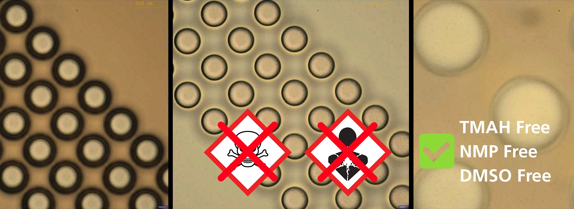
TMAH and NMP-free: An alternative to toxic stripping agents
Semiconductor manufacturing commonly uses chemical stripping agents to remove photoresists. While these agents are highly effective, they also pose significant health risks. One key criticism concerns additives like tetramethylammonium hydroxide (TMAH), a life-threatening substance that is highly toxic to humans even in small quantities, as well as N-methyl-2-pyrrolidone (NMP), which is also harmful to humans and toxic to reproductive health. Due to their potential hazards, both chemical substances are subject to the REACH Regulation in the European Union. It imposes specific restrictions on their use, with strict requirements for occupational safety and process safety in production.
»As part of the ›Green ICT‹ initiative, our partner in the chemical industry worked tirelessly on the development of an alternative stripping agent. From the very beginning, the goal was to find a solution that is completely free of TMAH and NMP, so that we are no longer exposed to highly hazardous substances during use. At Fraunhofer IZM-ASSID, we supported this development for several years and compared the resulting formulations with a reference agent under realistic conditions, in a comprehensive test«, Maksym Myndyk sums up, adding: »The new stripping agent was developed in three stages in total. The third-generation formulation now not only completely dispenses with the life-threatening substances TMAH and NMP, but is also free of dimethyl sulfoxide (DMSO).« Myndyk explains that DMSO is not critical in and of itself, but can act as a carrier and transport other potentially harmful substances into the body through the skin.
Impressive test results:
Faster processes and significantly less copper removal
To evaluate the performance of the new stripping agent, comprehensive tests were conducted at Fraunhofer IZM-ASSID. Their primary focus was on whether photoresist residues could be reliably removed and to what extent the underlying copper was corroded during the process. For this purpose, wafers with different surface preparations and metallization patterns were used to replicate typical industrial manufacturing conditions as closely as possible.
An industry-standard stripping agent was used as reference. That agent is frequently used in industry practice and has established itself as having fundamentally good cleaning performance. However, it contains approximately two percent TMAH and is therefore associated with known health risks. Additionally, it suffers from a relatively high copper removal rate. The results of the comparison are impressive: The performance of the new agent exceeds the original requirements for a TMAH and NMP-free stripping agent, as it not only reduces health risks, but also demonstrates significantly better process parameters.
Less copper removed
One key finding of the tests is the significantly reduced copper removal rate of the new stripping agent. This was measured in Angstroms per minute and compared with the established reference agent. The results showed that the new formulation can reduce material removal by a factor of about 20.
Myndyk explains why this is so crucial by referring to the wafer manufacturing process: First, a copper layer (seed layer) is applied to the wafer. On this layer, fine copper structures (so-called micro-pillars) are formed. The pillars are then selectively patterned using a photoresist. After plating, the photoresist must be removed, but the copper structures must remain intact.
Stripping chemicals attack not only the photoresist, but also the underlying copper. An excessive etch rate can cause the delicate microstructures to be damaged, or their geometry to be altered. The significantly reduced copper etch rate of the green stripping agent protects the integrity of these structures during production.
Significantly faster stripping
The new chemical also delivers impressive results in terms of process speed across a variety of applications. Tests were conducted on wafers with photoresist layers of varying thicknesses, including TOK photoresist in layers up to 70 µm thick and materials like AZ 10XT.
While the reference agent typically requires around ten minutes to completely remove such thick photoresist structures, the same result was achieved with the new stripping agent in as little as 90 seconds.

SEM images of a patterned wafer with plated pillars from the test series: V3AT with 70 μm TOK PR; results after 60 seconds at 70 °C
From left to right: After stripping, at 10x, 50x, and 150x magnification – focus on the seed layer. The complete removal of the photoresist is clearly visible. | © Fraunhofer IZM-ASSID

SEM images of a patterned wafer with plated pillars from the test series: V3AT with 70 μm TOK PR; results after 65 seconds at 70 °C
From left to right: Before stripping, at 10x magnification, and after stripping, at 10x and 50x magnification. The complete removal of the photoresist is clearly visible. | © Fraunhofer IZM-ASSID

SEM images of a patterned wafer with plated pillars from the test series: ATC4 with 20 μm AZ 10XT PR; results after 30 seconds at 70 °C
From left to right: Before stripping, at 50x magnification, and after stripping, at 50x and 150x magnification – focus on the seed layer. The complete removal of the photoresist around the 13 µm bumps is clearly visible. | © Fraunhofer IZM-ASSID
Surprising Success with Hard-to-Remove Dry Film
One particularly remarkable result emerged during testing with so-called dry film. These are laminated photoresist films used, for example, to build thick structures or in printed circuit board and advanced packaging manufacturing.
»After the plating process, the dry film layer on the wafers – which can be up to 230 micrometers thick – has been very difficult to remove. Neither the reference agent nor the first two iterations of the new stripping agent were able to reliably remove this film. With the third generation of the alternative stripping agent, this is now fully achievable – even if it still takes about 90 minutes. Nevertheless, the result represents a significant step forward, as it opens up entirely new application possibilities for lower-risk and more environmentally friendly chemicals,« explains Maksym Myndyk.
From Research to Application
The »Green ICT« research project, as part of which the work was commissioned at Fraunhofer IZM-ASSID, has now been completed. The positive and promising results of several years of developing and evaluating an alternative stripping agent demonstrate that the process is well worth the effort: »The new stripping agent combines several key advantages: In addition to achieving the goal of reducing the potential risk to humans, it is more environmentally friendly. In process applications, it can not only serve as an equivalent replacement for conventional agents containing toxic additives, but also outperforms the reference agent in terms of stripping times and copper removal rates,« Maksym Myndyk concludes. He also presented the results at the CMP & WET User Group Meeting in Halle (April 23 and 24, 2026).
»The new stripping agent offers several advantages: It is safer for operators and more environmentally friendly. It also delivers up to 85% faster stripping and a 20-fold reduction in copper removal.«
Dr. Maksym Myndyk, Wafer Cleaning Expert, Fraunhofer IZM-ASSID
The next step involves repeatability studies to bring the formulation closer to market readiness and actual industrial applications. At the same time, the results already point to its further potential: In future, it might also be possible to recycle the chemical used, for example through treatment and reuse, removing degradation products and replenishing specific additives. This could mean that the stripping agent not only offers short-term benefits for safety and process efficiency, but also long-term prospects for more resource-efficient and sustainable manufacturing processes.
The »Green ICT Competence Center« at the Research Fab Microelectronics Germany is a central point of contact for sustainable electronics. The Federal Ministry of Education and Research supports the project as part of the Green ICT initiative, which is part of the German government’s 2030 climate protection programme.
Network coordinator | FMD office |
Partners | Fraunhofer EMFT, Munich; Fraunhofer ENAS, Chemnitz; Fraunhofer FHR, Wachtberg; Fraunhofer HHI, Berlin; Fraunhofer IAF, Freiburg; Fraunhofer IIS, Nuremberg; Fraunhofer IISB, Erlangen; Fraunhofer IMS, Duisburg; Fraunhofer IPMS, Dresden; Fraunhofer ISI, Karlsruhe; Fraunhofer ISIT, Itzehoe; Fraunhofer IZM, Moritzburg; Ferdinand-Braun-Institut GmbH, Berlin; IHP GmbH, Frankfurt (Oder) |
Funding agency | Federal Ministry of Research, Technology, and Space (BMFTR); formerly: Federal Ministry of Education and Research (BMBF) |
Duration | 08/2022-01/2026 |
Website |
Editor’s note: The cover image for this article was updated on April 30, 2026. The original version had shown four pictograms. According to the safety data sheet, the chemical must still be labeled with two of these pictograms.