RealIZM blog series »Hardware Security« – Part 3
Reliable access to electronic components is of strategic importance for Germany’s future as the industrial hub in Europe. However, as more and more integrated circuit (IC) production is being moved to other continents, there is a growing risk that components will be compromised by backdoor functions that allow malicious actors to spy or otherwise tamper with the hardware.
To counter that risk, Fraunhofer Institutes and their German industrial partners are working on an innovative split manufacturing system for semiconductor production as part of the joint T4T project: »Tech-for-Trust: Distributed Manufacturing for Novel and Trustworthy Electronics«. The secure assembly and encryption of electronic systems in Germany is intended to prevent the espionage and theft of intellectual property in circuit design.
Heterogeneous integration – the combination of chip components from different technologies and production facilities – is attractive from both a technical and an economic perspective. It increases flexibility in chip production and reduces costs. At the same time, there are still many unresolved research issues like the development of multifunctional substrates or ways to increase trustworthiness and the hardware security of the overall electronic system.
One approach to increasing the trustworthiness of electronic components is to manufacture them independently of each other at different locations – including outside Europe – and then to combine them into a trustworthy joint system in Germany using assembly and interconnection technologies, such as die-to-wafer (D2W) or wafer-to-wafer (W2W) bonding. This can only work if the production design is laid out in such a way that a secure supply chain can be guaranteed in semiconductor production, even when there are numerous players involved.
The advantage of split manufacturing is that the manufacturers and suppliers of the electronic components involved cannot draw any conclusions about the overall system from the specific parts they are making. This makes copying impossible. Only the person responsible for the overall design has all the information about the complete system. For additional security, a cryptographic key can be integrated during production.
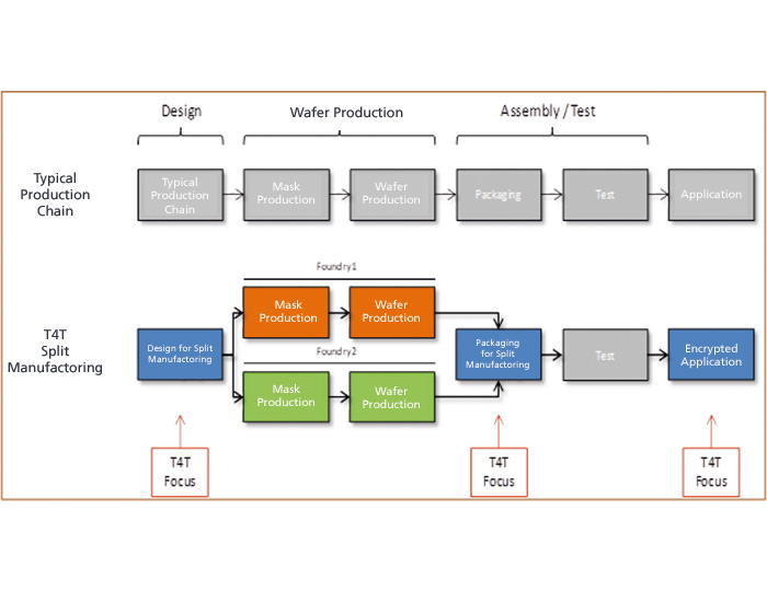
T4T distributed manufacturing and focus of the project | © Fraunhofer IZM-ASSID, Thomas Werner
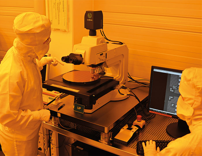
Fraunhofer IZM-ASSID and its project partners are working on various work packages in the T4T project, e. g. on the design methodology for split manufacturing, elements of the assembly and interconnection technologies and demonstrators. Most of the technological demonstrators are created using 300 mm processes.
The focus for Fraunhofer IZM-ASSID in the assembly and interconnection work is on stable process integration for very small contacts using different bonding technologies: Hybrid bonding with copper/silicon oxide contacts, nanowire interconnects and micro bumps. The aim is to realize the 5 µm contacts on a 10 µm pitch for all technologies – from the design phase to D2W bonding. The issue of different chiplet sizes is also being actively pursued in this project. All these technologies are necessary in the field of high-performance computing, which is characterized by very high contact densities.
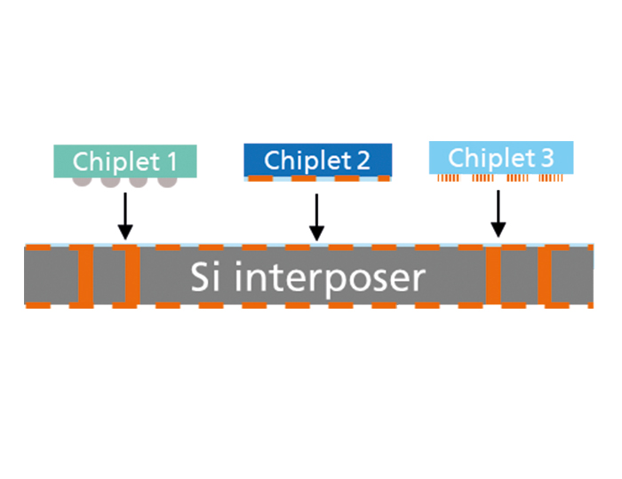
A schematic representation of a Si interposer with micro bump, hybrid bond, and nanowire chiplets | © Fraunhofer IZM-ASSID, Juliana Panchenko
Developing innovative demonstrators with hybrid bonding
Several demonstrators are being developed in the T4T project. One made by Fraunhofer IZM-ASSID is a technology demonstrator for chiplet integration on 300 mm Si interposers. At the same time, the Institute is participating in a demonstrator that is being developed with Fraunhofer IPMS at the helm. This demonstrator consists of a W2W hybrid bond stack of two wafers with encrypted memory for high-end applications with the highest demands on performance, reliability, and efficiency.
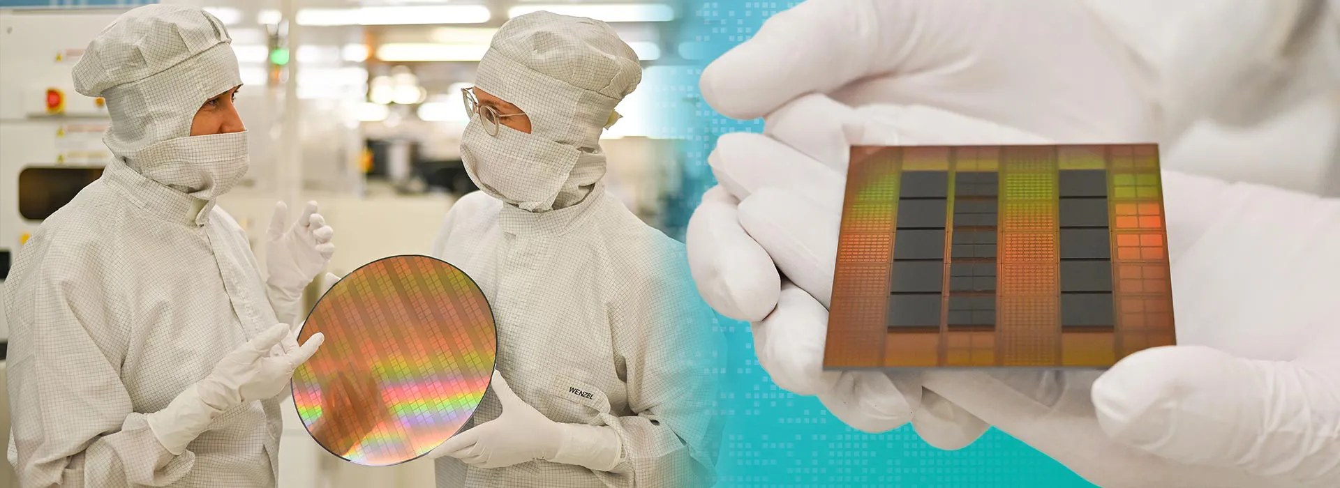
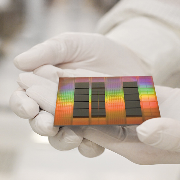
Left: Demonstrator: Assembled chiplets with ultra-fine copper hybrid bond contacts on a pitch of 10 µm | © Fraunhofer IZM-ASSID, Silvia Wolf
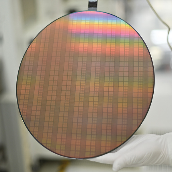
Right: Demonstrator: 300 mm Si wafer with high-density copper interconnects for chiplet integration as part of the “T4T” project | © Fraunhofer IZM-ASSID, Silvia Wolf
The chiplet demonstrator will illustrate that it is possible to combine at least two bonding technologies on a single Si interposer. It is expected that future chiplets will not come from a single foundry or have a uniform contact finish. Instead, they will have different surfaces. Both chiplets with soldered and DBI (Direct Bond Interconnect) surfaces will have to be interconnected and processed on interposers.
In addition, future chiplets will have different sizes, ranging from a few millimeters to centimeters. The chiplet demonstrator is intended to address the resulting issues. The plan is to bond and characterize the chiplets with different sizes and different surfaces (hybrid bond chiplet vs. nanowire chiplet, hybrid bond chiplet vs. micro bump chiplet) on a Si interposer. This is where Fraunhofer IZM ASSID is reinforcing its cooperation with the technology partner NanoWired, who supports the processing of nanowire chiplets.
The second demonstrator, a W2W hybrid bond stack with encrypted memory, illustrates how split manufacturing works when individual wafers are prepared in different factories. In this case, processing is carried out by Fraunhofer IPMS-CNT and Fraunhofer IZM-ASSID. The cryptographic encryption of the wafer is the responsibility of Fraunhofer IPMS-CNT and project partner SIJEDA.
Left: Hybrid bond interconnects with 10 µm pitch | © Fraunhofer IZM-ASSID, Prof. Dr.-Ing. Juliana Panchenko
Right: Demonstrator: 300 mm Si wafer with high-density copper interconnects for chiplet integration as part of the “T4T” project | © Fraunhofer IZM-ASSID, Silvia Wolf
Challenges and solutions for bond processes in split manufacturing
A prerequisite for the successful implementation of the split manufacturing approach is very good coordination between all parties involved. For the Fraunhofer IZM-ASSID team, it is crucial to know what the components from the various suppliers look like that need to be bonded using the available interconnection methods. Typically, a Si interposer for high-performance packaging applications is prepared with a DBI (or hybrid bond surface). This surface is critical if chiplets with DBI contacts are to be placed on it.
As soon as another electronic component is added, it must be checked whether and how reliability can be guaranteed in the long term. If necessary, the chiplets with the DBI contacts must be specially prepared, e. g. by thinning them, integrating them into the wafer line, and applying special pads to enable the bonding of other chiplets, e. g. with solder. The major challenge is to determine the exact sequence of the bonding processes and the required technologies and process steps.
When integrating chiplets with numerous contact points, the technological requirements must first be created in order to combine them in a bonding tool. It is not just the size of the chiplets that plays a role here, but also how the connection points are processed, and in which order the chiplets can be bonded to the interposer. In addition, the surface design of the interposer must be carefully thought out in order to be able to combine the different chiplets. Design optimization of the interposer surface is particularly important when chiplets of different sizes are used.
For bonding, a process sequence needs to be evaluated for placing larger and smaller chiplets, using various specialized pick-up tools. Especially for very large chiplets with an edge length of over 20 mm with very small joints, a homogeneous chiplet surface and the extremely plane-parallel alignment of the surfaces to be bonded are crucial. Even the smallest deviations can lead to considerable yield losses.
The T4T project demonstrates that this chiplet bonding technology for very small contacts is possible in Germany. Fraunhofer IZM-ASSID is working on developing robust and stable processes for small contacts (based on hybrid bonding, nanowires, and micro bump) for the D2W bonding process on 300 mm wafers. The T4T project paves the way for Laser Direct Imaging (LDI) patterning, which can be used to produce tiny structures down to 0.75 µm without additional masks.
Currently, neither standards for the production of highly integrated structures with chiplets and W2W processes nor design rules or assembly design kits (ADKs) exist. This is why Fraunhofer IZM-ASSID is working with Fraunhofer IIS-EAS on process flows for the design phase of distributed manufacturing and checking the design for its technological feasibility. The project consortium has also drawn up a roadmap for the »Conceptual design of a work-sharing ecosystem for advanced packaging in microelectronics«, meant specifically for Germany.
Outlook: Fraunhofer’s path to cutting-edge research in chiplet integration
Hybrid bonding is the gatekeeper technology that enables the reliable stacking of silicon chiplets at very high contact densities (pitches below 15 µm, contact diameters below 10 µm). This enables the construction of systems with high performance, high data rates, long service lives, and low latency. Fraunhofer aims to use this technology for 2.5D/3D assemblies with very small contacts. For larger contacts, both micro bumps and new nanowire technologies can be used successfully, offering advantages in terms of process costs and process temperatures.
The knowledge gained from the T4T project will be incorporated into the new Fraunhofer initiative »Chiplet Center of Excellence«.
Publications:
- Influence of Heat Treatment on the Quality of Die-to-Wafer Hybrid Bond Interconnects
- Investigation of Side Wall Loss for Development of 6 µm Micro Bumps for 3D/2.5D Integration
- Fine-Pitch Copper Nanowire Interconnects for 2.5/3D System Integration
- Cu nanowire fine-pitch joints for next gen heterogeneous chiplet integration
- Microstructure Development of Cu/SiO2 Hybrid Bond Interconnects After Reliability Tests
T4T »Tech-for-Trust: Distributed Manufacturing for Novel and Trustworthy Electronics«
T4T, or »Tech-for-Trust: Distributed Manufacturing for Novel and Trustworthy Electronics«, is a BMBF-funded joint project set up to prepare a secure supply chain through distributed (split) manufacturing in Germany.
Project sponsor:
VDI/VDE Innovation + Technik GmbH
Funding provider:
BMBF
Network coordination team:
Robert Bosch GmbH
Fraunhofer IZM-ASSID
Project partners:
ams-OSRAM International GmbH
AUDI AG
DISCO HI-TEC GmbH
NanoWired GmbH
X-FAB Dresden GmbH & Co. KG
X-FAB MEMS GmbH
Fraunhofer IIS-EAS
Fraunhofer IPMS
Fraunhofer IZM-ASSID
Leibniz-Institut für innovative Mikroelektronik
Technische Universität Dresden
SIJEDA GbR (assoziierter Partner)
SÜSS MicroTec AG (assoziierter Partner)
Duration & funding reference:
04/2022 – 03/2025 | 16ME0481
More information about Fraunhofer IZM solutions for the challenges of hardware security




Add comment