
 Maurice Laurent Haffner
 Tom Chojne
 Katja Arnhold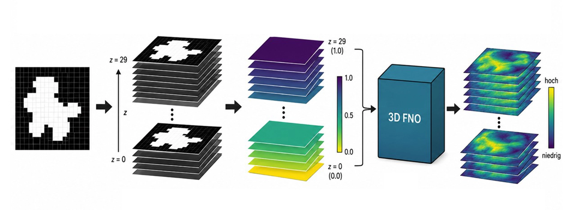
In harsh environments – such as in large energy parks – electrical and fiber-based sensors will soon reach the limits of what they can cope with. Lower performance, higher manufacturing costs, and a greater risk of electromagnetic interference limit their usefulness. In the »3DGlassGuard« project funded by Germany’s Federal Ministry of Research, Technology, and Space, industry partners and research institutions – including Siemens AG, Fraunhofer IZM, and TU Berlin – are working to overcome these challenges with optical sensor solutions for glass-core substrates and integrated optical fibers.
The trick is inverse photonic design: based on the predefined target parameters, algorithms automatically calculate three-dimensional microstructures in the glass that guide light with low losses. Traditional simulation tools would take months or years for the necessary calculations, which involve many individual iterations. This is why the consortium relies on AI-supported models to reduce simulation times from hours to seconds and enable fast, iterative design cycles.
In their chat with RealIZM, Maurice Laurent Haffner and Tom Chojne explain the goals of the research project, the potential of optical fibers integrated into glass, and the added value that AI-supported workflows offer in photonic design development.
In this article
- What Is Inverse Photonic Design?
- How Does AI Accelerate Photonic Development Processes?
- What Applications Are Being Developed in the 3DGlassGuard Project?
- Why Is Glass Becoming a Key Material for Next-Generation Photonics?
A Turbo Boost for Inverse Photonic Design
Inverse photonic design (IPD) is already being used in silicon photonics. Applying the method to ion-exchange waveguides is extremely challenging. Tom Chojne points out that ion-exchange waveguides are significantly larger than silicon chips and require enormous computing power. »Simulating the diffusion model of ion exchange takes ten hours, and another 24 hours for the light simulation,« explains the researcher. »Using conventional methods, the 1,000 required runs needed as the very minimum would take nearly four years.«
TU Berlin and Fraunhofer IZM are working together to drastically reduce this computation time. With the help of AI surrogate models such as Fourier Neural Operators (FNO), simulations are soon expected to be completed in seconds rather than hours. This requires extensive training datasets from conventional calculations as well as powerful computing resources.
TU Berlin is providing mathematical expertise and its GPU cluster for training the neural networks, while Fraunhofer IZM is using its 16-core CPU-based high-performance computer with approximately 2 TB/s of memory bandwidth to generate the training data, set up the optimization pipeline, and handle the integration of the AI models.
The simulation results are validated together, using agreed-upon metrics. As the project progresses, prototypes of the designed structures will be manufactured and checked against these results.
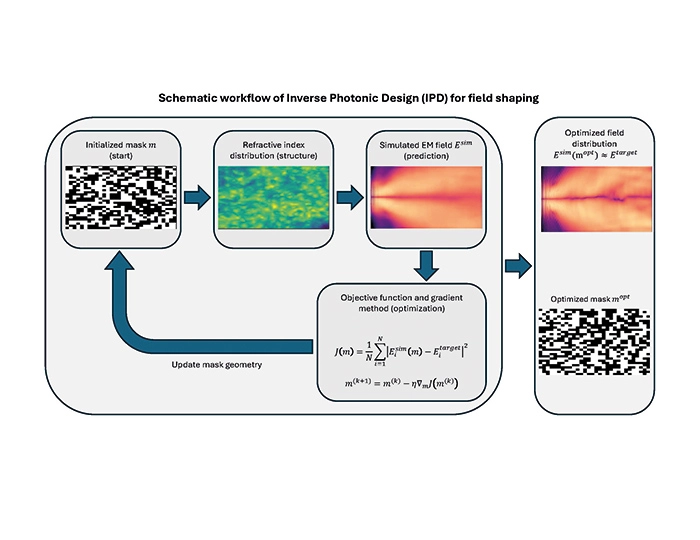
Schematic representation of Inverse Photonic Design (IPD) | © Fraunhofer IZM
A three-stage AI pipeline from material model to photonic design
The modular pipeline includes three components: the optimization algorithm, the diffusion module for calculating the ion distribution in the glass, and the photonic model for simulating the propagation of light waves in the glass. »The diffusion module is ready for use and can deliver the results of a single simulation in less than 30 seconds,« explains Tom Chojne.
Based on the gradients of both models, the algorithm iteratively determines how the design needs to be tweaked. To do this, it runs the simulation forward (diffusion and ion exchange) and then in reverse until all requirements are met.
AI doesn’t replace everything – it accelerates the design process
AI-based predictions require neural networks that have been trained on a large dataset. »We manually performed about 200 traditional simulations and consolidated them into a multidimensional data cube of about two terabytes. This ›data cube‹ maps the electromagnetic field for every grid position,« Maurice Haffner says about how the training dataset was created. The neural network learns to reproduce the data cube in a matter of seconds. The mean squared error must not exceed 0.1 percent. In practice, this means results that are almost as precise as conventional simulations – but available in seconds instead of hours.
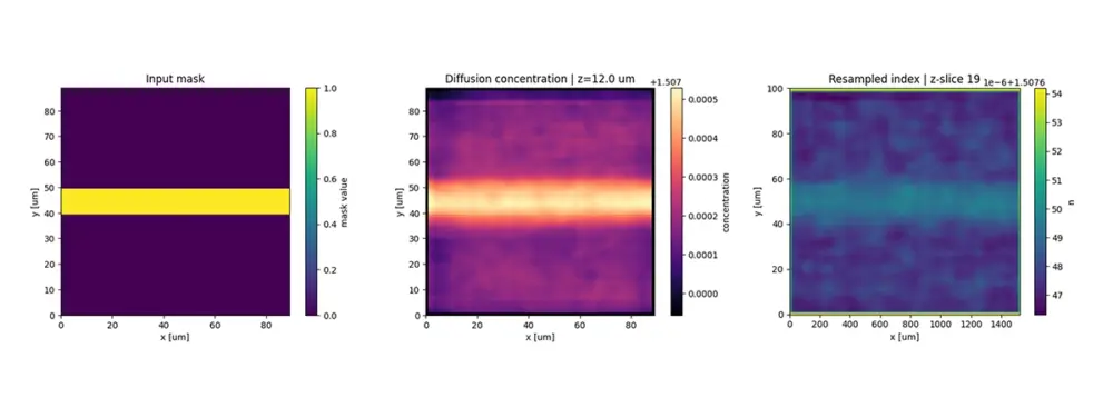
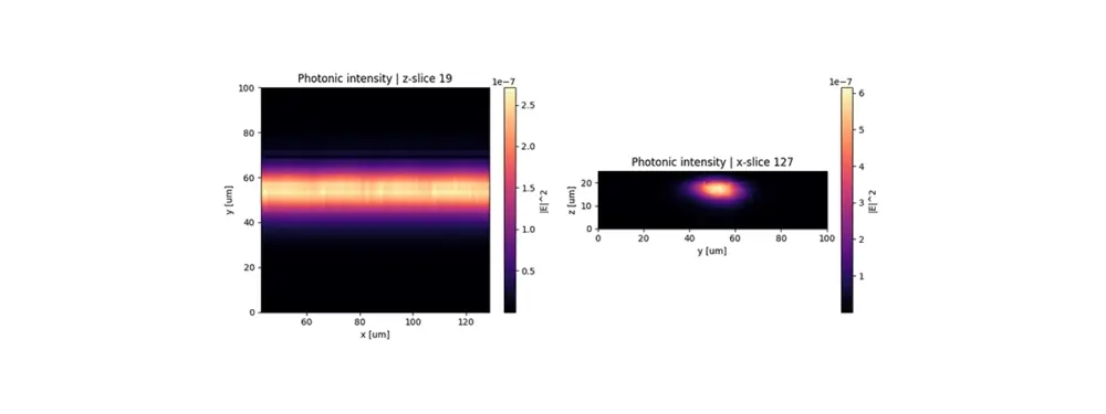
IPD pipeline: Forward propagation through a straight waveguide. The coupled pipeline generates a plausible guided photonic field for a simple straight waveguide. © Fraunhofer IZM
»With AI, we’re drastically shortening the entire computational process of inverse photonic design. In future, we want to use AI to quickly develop new design proposals and reserve conventional simulations only for the final iterations for validation.«
Maurice Laurent Haffner, »Optical Interconnection Technologies«, TU Berlin
Tom Chojne adds: »AI handles the rough adjustments, while traditional tools are only needed for the final fine-tuning.«
This hybrid workflow lays the foundations for efficiently integrating photonic components into glass – even for geometries that would be nearly impossible to manage using conventional methods. For the first time, three-dimensional optical structures can now be integrated into large-area, very thin glass substrates (< 1 mm).
»This enables new applications where high bandwidths, low latency, and electromagnetic robustness are critical – properties that conventional electronics alone cannot deliver,« Chojne summarizes. The pipeline for ion-exchange waveguides can also be applied to other types of glass, wavelengths, and different salt melt compositions during ion exchange.
From Simulation to Application: Demonstrators in the Project
At the halfway point of the project, key milestones have already been reached. »The validation of the core components – ion exchange and photonic simulation – has been completed,« Haffner summarizes. Initial preliminary tests with waveguide components and laser-inscribed waveguides have been carried out.

A splitter that evenly divides the light in the optical fiber into two channels, for example, to couple it into two different optical fibers | © Fraunhofer IZM, generated with Ansys Lumerical
The next step is the development of demonstrators. LightFab GmbH is working on an optical bending beam: on a patterned piece of glass, a free-swinging glass beam is excited by a magnetic field and measures the resulting current. Fraunhofer IZM is assisting with characterization, defining the parameters, and performing the metallization. In addition, Fraunhofer IZM is working on its demonstrator with 3D-printed lenses, built-in crystals, and a small optical bench
Another demonstrator is a TE/TM splitter that asymmetrically separates transverse electric (TE) and transverse magnetic (TM) signals. In cooperation with Siemens, an optical current sensor is being developed for power electronics applications to minimize the health and safety risks in control cabinets. The objective here is to enable galvanic isolation in current sensors. This means that the circuit to be measured is separated from the circuit required for measurements. Until now, this separation was achieved using resistors through which very high currents flow, generating heat. Optical fiber technology promises greater efficiency and increased safety.
The TE/TM splitter is being developed using inverse photonic design. »The other components are still designed using conventional methods,« explains Haffner. »Looking ahead, we want to replace them with inversely designed components that are more compact, enable higher transmission, and operate more efficiently overall.« Using the Lego principle, photonic components can be adapted for other applications.
Glass as a Versatile Substrate for Next-Generation Photonics
In current research, glass is primarily used as a carrier substrate.
»However, glass is suitable not only for packaging, but also for creating optical pathways directly within the substrate.«
Tom Chojne, »Optical Interconnection Technologies«, TU Berlin

Manufacturing process for optical fibers integrated in glass | © Fraunhofer IZM
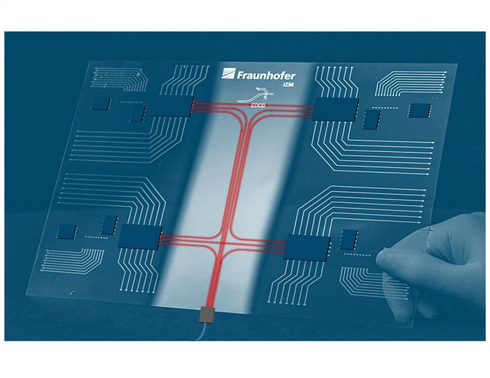
Electro-optical Circuit Board (EOCB) | © Fraunhofer IZM
Conventional semiconductor chips are reaching their physical limits in terms of miniaturization and increasingly dense packaging. A forward-looking solution is chiplet architecture: multiple specialized chips are combined on a single board and interconnected. »Communication between these chiplets via integrated optical fibers is significantly more efficient than via semiconductors,« says Haffner. Core components of this concept are photonic components such as wavelength-selective splitters, which are optimized using inverse design.
The goal is to deploy photonic connections directly in data centers in the medium term to accelerate communication between chips and make it more energy-efficient. In the long term, this opens up entirely new fields of application beyond traditional electronics – from ultra-fast optical backbones in data centers to sensor-actuator systems embedded in glass for smart grid and IoT applications.
Further reading: Co-packaged optics for data centers
Photonic connections can play an important role in the energy-efficient transmission of large volumes of data in data centers. Learn how co-packaged optics bring optical and electronic components closer together and explore the challenges involved in »Faster, Higher, Stronger: Why Co-Packaged Optics are a Game Changer«.
More on glass as a platform for integrated photonics
Discover how glass can serve not only as a platform for integrated optical waveguides, but also as a basis for photonic packaging in »From Prism to Glass Interposer: UNESCO Commemorative Year Marking the 200th Anniversary of Joseph von Fraunhofer’s Death and Glass as a Key Material in Integrated Photonics«.
3DGlassGuard – Safety through Photonic System Integration in Glass Films
Project Duration | 05/2024 – 05/2027 |
Grant Reference | 13N16851 |
Funding Agency | BMFTR |
Funding Amount | €4.67 million (69.3% funded by the BMFTR) |
Project partners | Siemens AG (project lead), Sea & Sun Technology GmbH, Contag AG, LightFab GmbH, Fraunhofer IZM, and TU Berlin, as well as Schott AG (associated partner) |
Project website |
 Jana Rückschloss
 Franziska Maisel
 Theresa Aigner
 Alexandra Morozov
 Fabian Pranter
 Enrica Theuke
 Susann Thoma
 Dr. Michail Symeonidis