Everywhere in the world, the bandwidth of Ethernet networks keeps growing. This extremely rapid growth is powered by the great progress made in many areas involved, such as video, AI, HPC, and 5G. The operators of data centres and research organizations are now looking for solutions with significantly better power efficiency and performance rolled into one. They are placing their hopes into novel concepts to keep up with new technological needs and standards.
One of the initiatives pursued by them is co-packaged optics, a promising technology that has lots of advantages over optical transceivers, including better thermal management, power consumption, bandwidth, and many more. RealIZM has met Bogdan Sirbu, a researcher at Fraunhofer IZM, to speak about the need for and challenges of co-packaged optics, the technology’s readiness, and future developments in datacentres and beyond.
Can you give us a brief overview about co-packaged optics (CPO)? What are their advantages compared to conventional solutions?
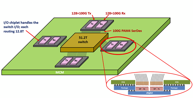
Bogdan Sirbu: We see certain applications, such as video, AI, HPC, or 5G, driving the demand for more bandwidth, higher performance, and just bigger-scale solutions, with a major focus on power efficiency for the networking solutions in data centres. With the current state of the art, the most popular switching solution in data centers has a throughput of 12.8 Tbps. It consists of a big unit switch system that usually has 32 pluggable transceivers with 400 Gbps each per transceiver. Assembling such transceivers is quite straightforward: It’s a small PCB, for which the silicon photonic chips are assembled using high-speed SerDes I/O traces. On top of that PCB, there is typically a silicon bench with the assembled electrical-optical conversion components, such as lasers and PDs, together with their driving electronics. The current technology roadmap includes HF channels operating at 100Gbps, but then we are already facing serious performance and reach limitations and the issue of massive power consumption.
Co-packaged optics is an up-and-coming technology that addresses these challenges created by small form factor pluggable optical transceivers. With it, you can bring optics as close as possible to the silicon switch or ASIC to achieve higher bandwidths and better energy efficiency. By bringing the active devices and the optical transceivers onto the same package, you can reduce the physical distance between components and keep electrical traces to the absolute minimum length, while reducing power consumption of the switch and having significantly higher I/O counts.
Can you use co-packaging only in data centers, or does it work in other applications as well?
Bogdan Sirbu: I think the main application will be data centers, where the goal is to achieve higher bandwidths while reducing power consumption. This can be achieved, alongside other strategies, by bringing the optics closer to the switches. The roadmaps are defining a progression of system packaging options to support next-generation equipment. They are predicting the trend of moving the optics closer to the switch starting from the edge of the PCB, as is used in the current, state-of-the-art transceiver packaging schemes, evolving to the eventual integration of the optical engine into the switch chip itself.
The current goal is to deploy co-packaged switch modules in data centres for a throughput of 51.2 Tbps in 2023 and 102.4 Tbps by 2025. The first proofs-of-concept shooting for these ambitious goals are already being reported. IBM was the first company that showed the potential of co-packaged modules, and now we’re seeing some demonstration units from the Big Five (Alphabet, Amazon, Facebook, Apple, and Microsoft) for 51.2 Tbps co-packaged switches.
Could you tell us more about research projects for co-packaged optics?
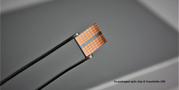
Bogdan Sirbu: One example I can think of is the H2020 L3MATRIX project [1]. On this project, we developed a 2D matrix of 64 different transceiver and receiver cells, achieving high radix and getting an extended bandwidth of 25 Gbps per channel in single-mode fibers and waveguides with low latency. The active components, such as lasers and photodiodes, were integrated directly into the silicon photonics. The packaging of these 2D photonic arrays in a chiplet configuration was developed using a vertical integration method, for which the optical interconnect matrix was flip-chip assembled on top of a CMOS chip with 2D vertical fiber matrix coupling. Finally, we successfully tested the individual cells to show the feasibility and functionality of the module. The result is a 10-fold reduction in power consumption (to the 3pJ/bit) compared to conventional technology, a great reduction in port-to-port latency into the 10-20 ns range, and lower costs of more than 40%, primarily from electrical power consumption and total cost of ownership.
Where do you see the biggest challenges in implementing of co-packaged optics?
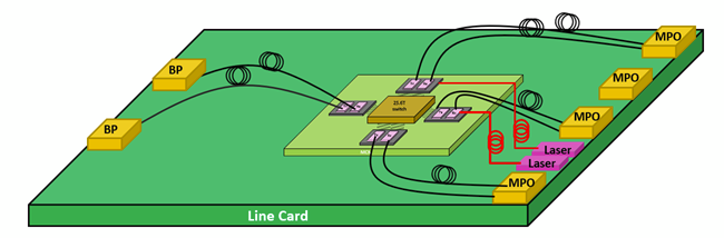
Bogdan Sirbu: One of the main challenges of this technology concerns optical connectivity. It increases the total fibre count per unit and simultaneously adds complexity in fibre routing for each co-packaging optics engine. In the current prototypes, one optical engine is placed in the middle and surrounded by these modules in the four cardinal directions, south, west, east, and north, connected by fibre to the edge of the PCB. Over there, they are terminated on MPO connectors. That results in different lengths of fibres, making the routing very complex. A more promising alternative solution, which should decrease the complexity of the optical routing, could be based on a common optical waveguide platform within the PCB.
Another challenge is heat dissipation: The optical engines are assembled very near to the ASIC or to the switch, which usually require considerable amounts of power, and most of this power is dissipated in the form of heat. The optical engines contain temperature-sensitive electro-optical components, such as lasers, photodiodes, or modulators, all of which require stable and carefully controlled temperatures to perform optimally. Therefore, heat management in such co-packaged solutions might be problematic.
Could we use glass photonics also for co-packaged optics?
Bogdan Sirbu: Yes, glass can be also used as a support platform for these co-packaged solutions. By definition, the optical connectivity between optical engines can be done via glass waveguides or on polymer waveguides processed on such glass substrates. The current glass waveguide technology is not applicable with respect to the flip-chip assembly boundaries of Silicon photonic integrated circuits on glass interposer for high volume manufacturing. Under the consideration of such assembly boundaries polymer waveguides on glass substrate are suitable and promising for low cost manufacturing. Nevertheless, the most mature technology for such co-packaged solutions is still silicon photonics as an interposer.
What is your opinion about the general development of this business area?
Bogdan Sirbu: The network providers, the data centre and network infrastructure companies, are moving towards co-packaged optics. The Big Five are showing lots of interest in this area, as they identified the problem with server connectivity inside data centres, which might require more advanced solutions. The data centre connectivity is based on different hierarchies of switches, which are mostly connected to each other using optical fibers with transceivers. It requires a huge space and vast amount of fibres. That is where Fraunhofer IZM comes into play with its knowhow and ability to find a smart solution and satisfy the market players’ needs.
Who are you cooperating with?
Bogdan Sirbu: We are teaming up with companies interested in the development of the technology. We are mostly active in design, integration and packaging. However, we have limited capabilities to develop the entire system on our own or to fabricate e.g. silicon photonic chips. For that, we are relying on some key partners who can provide complementary technology to ours. A good example is our consortium within the L3MARTIX project.The technology that I mentioned before was developed in a cooperation that included not only Research and Technology Organizations, such as Aristotelio Panepistimio Thessaloniki, Universitat Politecnica de Valencia, or University College London, but also industrial partners, such as ams AG, IBM Research GmbH, Bright Photonics BV, and DustPhotonics Ltd.
Are you working with any SME?
Bogdan Sirbu: SMEs are indeed active in this field. They’re doing research and development in pluggable transceivers. Their long-term focus is to include co-packaged photonics in their portfolio. But most interest today still comes from the large data centres and network equipment providers companies, like the mentioned Big Five.
Are there any other active or planned projects in the field?
Bogdan Sirbu: We are also working towards enabling high-volume manufacturing for pluggable transceivers. For example, the H2020 MASSTART project will turn Europe into a producer of next-generation technologies, improve cross-fertilization between photonics and other areas of technology, and strengthen Europe’s leading position in the global photonics industry.
When we will see co-packaged optics coming to the mass market?
Bogdan Sirbu: Right now, we are using 12.8 Tbps switches that could easily be reached with pluggable transceiver modules. However, we are already at the scalability limit for transceiver-based switches, and co-package optics is one of the possible solutions which could reach the market in 2023 with a throughput of 51.2 Tbps. The traditional trend in switches, i.e. doubling the throughput of the components, will most likely hold true going forward. However, it is still unclear whether co-packaged optics technology is a long-term solution or simply an interim step towards optics being directly integrated into high-performance chips.
[1] K. Papatryfonos, D.R. Selviah, K. Hasharoni, B. Sirbu, H. Oppermann, T. Tekin et al.: “Co-Package Technology Platform for Low-Power and Low-Cost Data Centers“, MDPI Appl. Sci. 2021, 11(13), 6098
L3MATRIX project is funded under the EU Research and Innovation programme Horizon 2020 with Grant Agreement Nr. 688544.
MASSTART project is co-funded by the Horizon 2020 Framework Programme of the European Union with Grant Agreement Nr. 825109. https://cordis.europa.eu/project/rcn/219912/factsheet/en
MASSTART project is an initiative of the Photonics Public Private Partnership. www.photonics21.org


Add comment