According to experts, heterogeneous integration increases not only the degree of miniaturization, but also the functional density of microelectronics. This approach could be a solution for companies in a vast range of industries, vying for competitive advantages in their market and trying hard to stay cost-effective.
The obvious question is: How to access this technology? The researchers at Fraunhofer IZM are working together with industry and government partners to develop an industry-wide heterogeneous integration ecosystem. Erik Jung, a senior researcher in the business developer department at Fraunhofer IZM in Berlin, tells RealIZM more about these efforts.
Would you give us a quick introduction to »Heterogeneous Integration«? What are the competitive advantages of this technology?
Erik Jung: Heterogeneous integration is the opposite of what we call monolithic integration. This approach puts as many functionalities as possible into one single chip, which is manufactured in one seamless process. It turns out that this approach provides the best scaling prospects, meaning the lowest cost per area. But with the complexity involved in it, it’s only feasible for large fabrication runs, and it’s also limited to functions that can be built together in the same fabrication process.
Heterogeneous integration, similarly, uses special integration techniques to bring the various functional blocks together in a form factor that is not unlike a System on Chip (SoC). However, it gives you substantially more freedom when it comes to selecting the functionalities you would like to integrate. This is achieved by the fact that you pick the best processes for a given functionality. Just think: For optical functions you would prefer another technology flow than you would for a memory or microcontroller device. Then you split the manufacturing form factor – typically, this would be a wafer – into the individual functions, like the dice. By bonding these individual functional blocks, which are small pieces of hardware on their own, to a common silicon or glass substrate, the respective functions are merged together.
Therefore, you do not use bulky organic substrates anymore. Instead, you go for high-density integration techniques. In the end, you can achieve a form factor that is as near as one would be able to get using System on Chip (SoC), but with much larger flexibility with respect to the functions you can integrate.
Heterogeneous integration is actually one way of implementing this kind of complex system. That is why most of the research institutes and most of the commercial players are looking into this type of additive integration, with IZM right at the forefront among them.
When we are talking about heterogeneous technologies, what is the current state of the art?
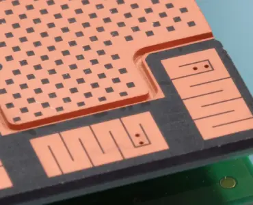
Erik Jung: Ultra-fine-pitch flip chip bonding is the pacesetter for this kind of small form factor integration. So, having backside contacts of the individual functional blocks and mounting everything on a small silicon carrier with through-silicon via – which we dub high density interposers – was actually the central key for the success of heterogeneous integration, as it brought together of those functional blocks. Using flip chip technology, you can get to a silicon fill factor close to 100% compared to the 40%…50% you get with organic high-density substrates. Now if you think ahead, you will be not limited anymore to just this kind of 2D integration. You can go up to 3D stack integration. It depends on, for example, whether you need media access or whether you need optical access or whatever.
Which developments has Fraunhofer IZM contributed in the field of heterogeneous integration?
Erik Jung: The main mission of the Fraunhofer IZM is integration towards fully functional systems. This trend towards heterogeneous integration thus fits very well into our portfolio. Now, we can use sensor chips, for example, communication chips, or control and number crunching chips for doing some upfront calculations of the sensor parameters, prior sending the data to cloud storage. This is all now possible on an extremely small form factor by using our 3D integration techniques with 300-millimeter through-silicon via capabilities. Moreover, we have a full range of capabilities in rerouting contacts on bumping and flip chip assembly techniques.
We are even going beyond the current state of the art by looking into technologies that could master the challenges typical in a small contact flip chip assembly, e.g. working with chips of different thicknesses.
The approach we are looking into is using so-called reconfigured wafers. We align the individual building blocks of a system in package (SiP) onto a temporary carrier and, by a type of compression molding process, we give them a new external shell. Then, by using our rerouting technologies, coming from wafer level packaging, we have now the ability to interconnect those chips to each other with extremely small distances and even use them another time for a stack assembly with through-mold vias, instead of the through-silicon vias I mentioned. That gets you to a very small, very functional, and fully integrated device. This SiP approach merges all of these heterogeneous functionalities into one tiny package. In addition, in order to lower manufacturing costs for these heterogeneous integrated packages, we have also been expanding the manufacturing sizes from the 200-millimeter wafer to a 300-millimeter wafer. We have pushed this forward idea to full panel level packaging size, which brings us from 457 to 610 millimeters panel sizes. That gives you a substantial scaling factor with considerable cost benefits as well.
What are the biggest challenges IZM is currently facing?
Erik Jung: There are some technological questions, e.g. how to deal with lots of different functionalities which all require a different set of design guidelines, or how to interconnect and how to interface with the other elements in a heterogeneous concept. Our design team is now put on the spot much more than ever before. In addition to this, testing has become extremely critical, because testing typically works only in one domain: You go either for DC testing or for digital or analogue testing, but you typically do not have an easy way of combining these various tests, let alone include optics and fluidics.
What technological solutions can Fraunhofer IZM offer?
Erik Jung: The technological capabilities at IZM relate to silicon-based heterogeneous integration, using through-silicon via substrates with high-density interconnects. That combines the various functionalities, so these small tiny hardware blocks fit onto this one carrier substrate either by flip chip technology. Or we can go for hybrid bonding, but this requires all the contacts from the front of the functional chip to be on the backside.
We also have the ability to move to high-density wafer level wire bond interconnects. In most cases, this is not our preferred option, because you lose the advantage of the form factor. Wirebonding needs some space to the side of the chip, limiting the scale advantage we could realize otherwise. This notwithstanding, it is doable especially if you only have access to a small number of singulated chips. In that case, it is an approach that still gives you access to cutting-edge implementations.
In addition, our approach for panel level and wafer level embedding is a clear asset, particularly if you are looking for slightly less challenging requirements or low cost manufacturing.
Can you tell us more about the current heterogeneous integration projects at Fraunhofer IZM?
Erik Jung: The sheer variety of our projects is astonishing. We might start with cooperation projects on a European level and eventually move them over into industry. Then industrial customers tell us about their needs, and we assist them with finding the right implementation, whether it is in the automotive industry or the healthcare sector. Let’s speak about some examples from medical electronics:
One of the most interesting cases is an European project we conducted together with a company called NXP. The main idea was to put together not only electrical functionalities, but also biological sensing capabilities, using wafer level technology. The sensing chips with their electronic readout circuitry were combined into a type of functional SiP, which brings together a versatile set of biological sensing and electrical interpretation features. We then added some micro-fluidics for the subsequent integration into a cartridge format. This eventually led to a global initiative on panel level packaging which has other major players cooperating.
Another flagship project we are involved on the European level is the Human Brain Project, where we stack various functionalities on top of each other by 3D integration to mimic the performance of the human brain.
You have been working with other technology organizations to develop a technological roadmap for heterogeneous integration. Can you tell us more about that initiative?
Erik Jung: The roadmap initiative was triggered by the IEEE, the world’s largest association of electrical engineers, including several of the biggest players in the industry.
They have seen the need for creating a roadmap that tackles the future challenges of heterogeneous integration. Industry members are typically looking for technology announcements for the future, because they have to decide where they want to put their investments. They need to know most, if not all of the challenges they might be facing in the near future. The big players in the IEEE like Intel, for example, came up with the idea of a joint roadmap to make sure that we don’t miss any opportunities at this pre-competitive stage and make sure that we have a common impulse for the industry towards this very promising approach in future system integration.
As part of that heterogeneous integration roadmap process, several technology working groups were formed and assigned their respective tasks in the matrix, which address possible areas of application from medical, safety, and security to automotive, power, and so on. IZM, in this case, has taken over a leading role for the SiP integration part of the roadmap, with a list of prospective technologies that the industry can use as a toolbox for the near future.
How would you envision the future of heterogeneous integration? What is the next step after SiP technology?
Erik Jung: From where I’m standing, heterogeneous integration in its various flavors will stay with us for a long time. If you look back at the history of electronics, you can see that functions were successfully included into integrated circuits, but there was not so much change on the level of the systems as a whole. When you had a function shifted to the chip, you just added more functionalities on the outside. Now, we can put those additional functionalities more and more into a form factor that is not unlike on-chip integration, but gives you more flexibility. This approach opens up the playing field for a huge number of product innovations.
I believe it will eventually become the basis for our electronics industry, even though there are some really disruptive concepts on the horizon.
For example, we are noticing the disappearance of a couple of functionalities of chips or modules brought about by the advent of latency-free communication. These might be shifting more to the outer world, for e.g. distributed sensors in your vicinity, and you can communicate with them, instead of having to track parameters directly on your own device.
Furthermore, we are seeing other conceptual approaches in bioelectronics, as I mentioned before, like the Human Brain Project, which is replicating the normal structures of the brain by means of fully silicon integration. Some research institutes are even looking already into having live neurons, which can be part of such an electronics system.
Some institutes are also discussing quantum technologies, such as quantum computing or quantum sensing. I do not see many openings for easily implementing heterogeneous integration in the currently favored concepts involving cryogenic tanks. Still, there are some aspects on the way, which are promising to have quantum power at room temperature. That would give us even much more opportunities for more components and functionalities to integrate.
This interview was conducted by Yulia Fedorovich and Marieke Lienert from Fraunhofer IZM Marketing & Business Development department.


Like!! Great article post.Really thank you! Really Cool.