
Did you know that miniaturized microchips and novel smart devices tend to depend on one almost invisible ingredient: the substrates? These high-resolution and finely structured substrates are the key to modern electronics.
Ruben Kahle, research associate in the »Embedding & Substrate Technologies« group at Fraunhofer IZM, invited the RealIZM blog team to an exclusive video tour of the Berlin cleanroom. We packed our camera, swapped our office clothes for protective suits, and entered the world of the cleanroom.
Follow us! You too can gain fascinating insights into the world of HDI substrates and discover their versatile applications.
Substrates are the link between the structures of the printed circuit board and the inputs and outputs of high-performance microchips. They form the bridge between the micro world of printed circuit boards and the nano world of the semiconductor industry. Similar to the foundations of a house, substrates act as the base layer of a printed circuit board and are essential for microchips to do their job of processing data.
With the ongoing miniaturization of electronic components and the ever-increasing demand for artificial intelligence (AI) networks, creating printed circuit boards and chips is also becoming more and more complex. Electronic products and applications with higher-quality technical functions now come with tougher requirements such as their energy efficiency, ways to reduce costs by saving materials or space, and ideas to conserve precious resources.
The abbreviation HDI stands for High Density Interconnect(ion). The use of HDI substrates requires semi-additive processes, stacked µvias, and dielectrics that are particle-filled or unfilled.
As a pure-play foundry, Fraunhofer IZM offers comprehensive solutions from a single source for research and development – from layout design and material selection to production. »With the technology portfolio at our disposal, we can manufacture substrates with glass cores and organic IC substrates and create the redistribution layer on molded panels (FOPLP),« explains Ruben Kahle, describing the options available at Fraunhofer IZM.
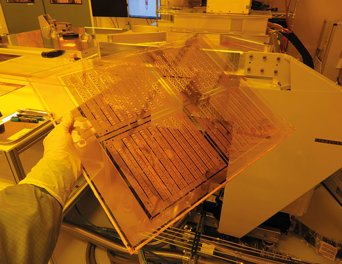
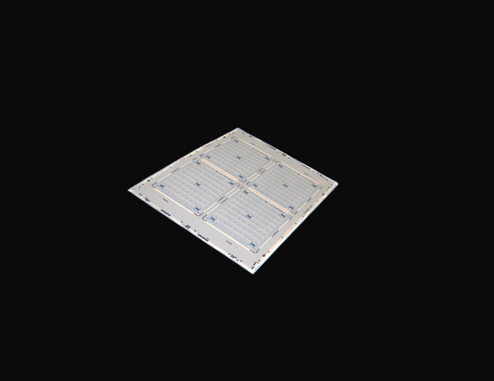
Left: Glass core substrate (GCS) with a high-density structured copper test layer of 2mm glass for demo purpose
Middle & Right: Assembly sequence of dies into cavities on full substrate size 510mm x 515mm prior to embedding
© Fraunhofer IZM
The development of HDI substrates is primarily driven by the wishes of clients and advances in wafer technology. “The design of HDI substrates and the production process in our line of work are subject to constant change,” explains Kahle.
»Substrate design follows chip design. The number of layers and the number of necessary contact points, conductor tracks, and connections in and out of the substrate is increasing. This means that we therefore depend on software solutions that can take a holistic view of a system or package.«
In addition, production processes for conventional PCB technology are reaching their physical limits. When producing fine structures in copper, traditional processes can only be miniaturized to a certain point. This is why the process chains for HDI substrates and their subsequent generations are turning to semiconductor technology, e.g. PVD sputtering, damascene technology, or photopatternable dielectrics. However, these processes work on a specific small and round format (wafers with diameters of 200 mm or 300 mm).
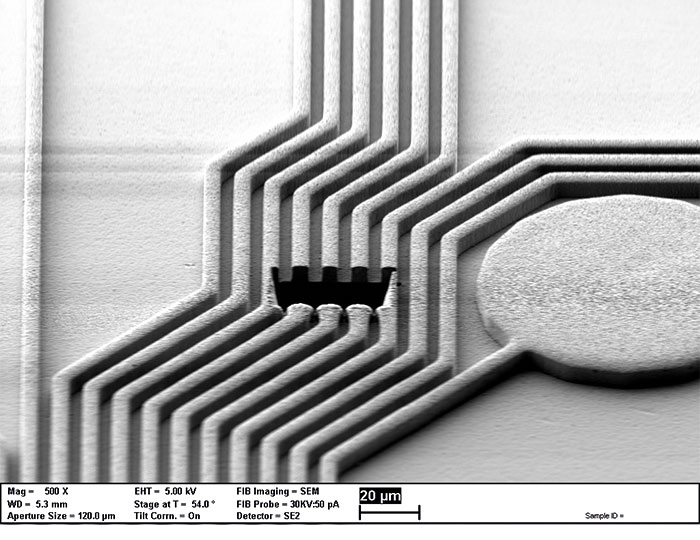
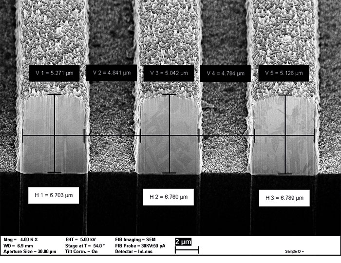
Left: Redistribution layer (RDL) line band 5 µm L/S with a 50 µm diameter contact pad
Middle: Focused ion beam (FIB) cross-section of a redistribution layer (RDL) 5 µm L/S
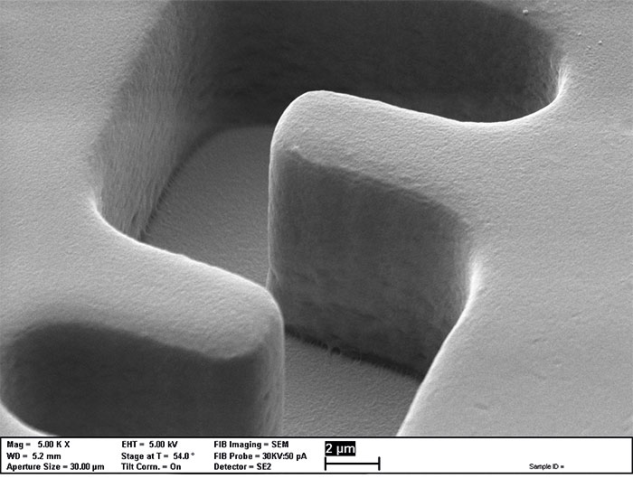
Right: Scanning electron micrograph (SEM) bird view of a 5 µm L/S photo resist after development, film thickness 7 µm
© Fraunhofer IZM
SEM bird view of a 5 µm L/S photo resist after development, film thickness 25 µm © Fraunhofer IZM
»We have to scale each individual step in the production chain up and adapt it to a large, rectangular format (panel),« Kahle says about the challenges of implementing this. At Fraunhofer IZM, the machines and materials in the cleanroom are designed for the production of HDI substrates in order to handle the 510 mm x 515 mm and 610 mm x 457 mm (24“ x 18”) formats or the quarter-sized 303 mm x 227 mm (12“ x 9”).
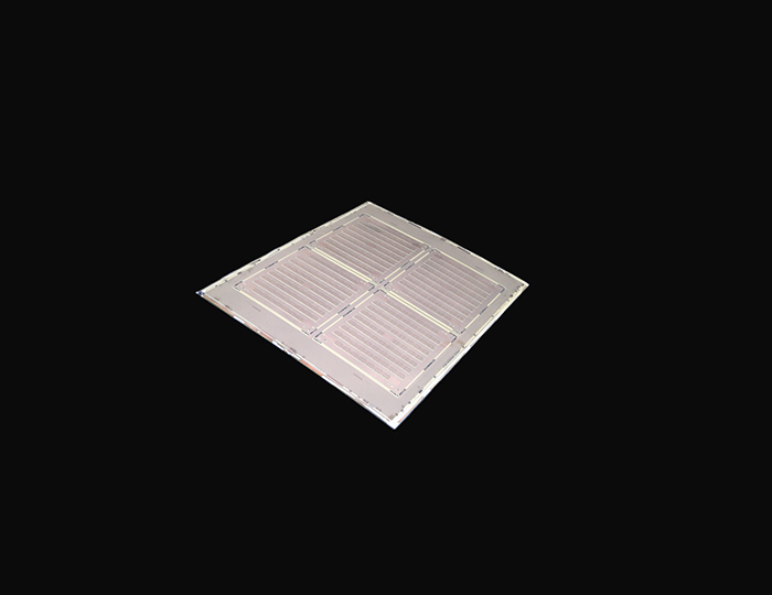
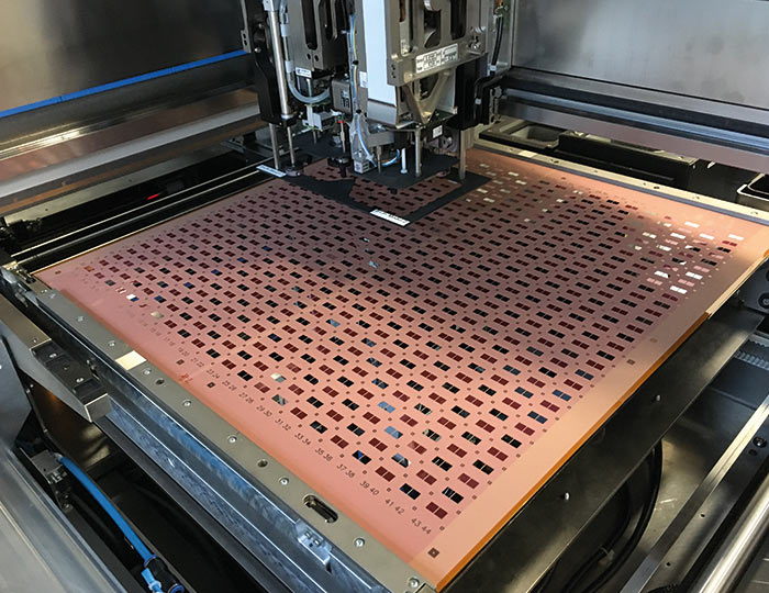
Left: 610 x 457 mm substrate with embedded chips made in collaboration with project partners on the CHARM project
Right: 610 x 457 mm substrate with multilayer wiring
© Fraunhofer IZM | Francis Viebeck
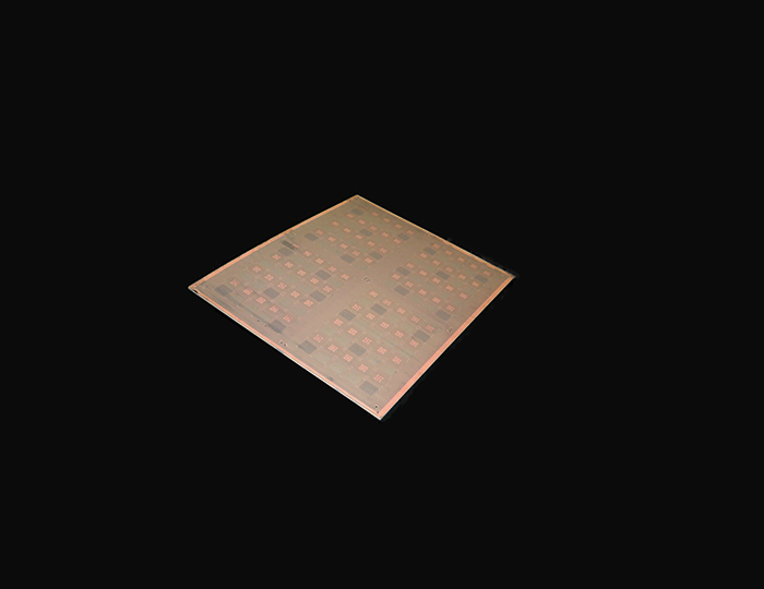
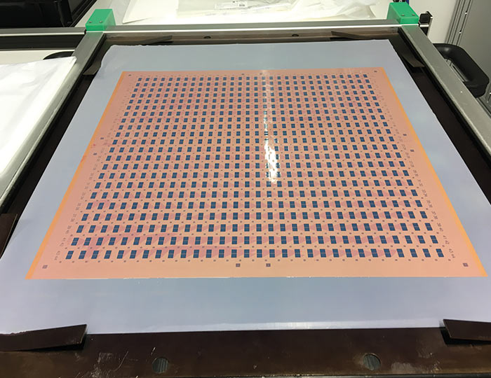
Left: 610 x 457 mm substrate with embedded chips after adding the first redistribution layer
Right: 610 x 457 mm substrate with structured resist after lithography for quality control
© Fraunhofer IZM I Francis Viebeck
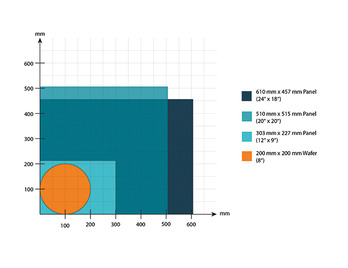
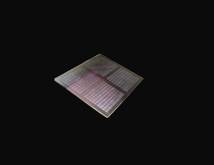
Graphic panel size HDI substrates © Fraunhofer IZM
»Depending on our customers’ specifications, we manufacture prototypes and small series with HDI substrates from 5 µm line/space upwards. For research and development, we are also able to go below 5 µm line/space to a current minimum of 2 µm line/space. We are currently at an experimental stage.«
The use of HDI substrates has many advantages that make them a preferred choice in modern electronics. Substrates not only offer increased packing density and improved electrical performance, but also enable the flexible design of complex circuits.
- Compact design: Higher packing density thanks to finer conductor tracks, significantly smaller vias, and more layers. Ideal for portable devices and applications with limited space.
- Improved electrical performance: Shorter signal paths reduce signal loss and increase signal speed.
- Increased design flexibility: Complex circuits can be integrated efficiently because vias can be stacked (any layer technique).
- Reliability: Fewer solder joints and connections reduce potential failure points.
- Thermal management: Improved heat dissipation through thinner materials and optimized layer arrangement.
- Use of modern components: Enables the use of smaller, more powerful ICs and advanced chips (e.g. BGA, CSP or bare dies).
- Adaptation to high frequencies: Ideally suited for applications in telecommunications (5G), IoT devices, and high-speed communication.
Printed circuit boards with high connection densities are used in consumer electronics such as smartphones, digital cameras, laptops, and tablets, among other things. USB-C and Thunderbolt ports benefit from the high-speed data transmission of HDI printed circuit boards.
Modern driver assistance systems are based on radar and camera systems that also use HDI printed circuit boards. Thanks to their excellent signal integrity and durability, HDI PCBs are also suitable for applications in the aerospace and defense industries, e.g. in radar systems, GPS, and other navigation systems.
Medical engineering also offers a wide range of possible applications, e.g. for making miniaturized ultrasound devices or portable heart rate monitors.
Reference project CHARM: Electronic Systems for Extremely Robust IoT and AI Applications
As part of the CHARM project of the ECSEL joint initiative, Fraunhofer IZM and its project partners developed solutions for the industrial internet of things (IoT) that work reliably even in harsh industrial environments. In this project, solutions were developed for six use cases in condition monitoring, predictive maintenance, and real-time quality assurance, including IoT applications in the mining sector. The subproject was focused on developing radar sensors that can enable mining machines to operate autonomously in »digital mining«.
Fraunhofer IZM contributed its expertise in process development for the reliable integration of silicon components into substrates and their contacting to the project. In collaboration with AT&S, an embedded computer module was developed. In addition, experiments were carried out to produce the rewiring of microelectronic components (high density wiring) in assembly substrates using advanced structuring processes.
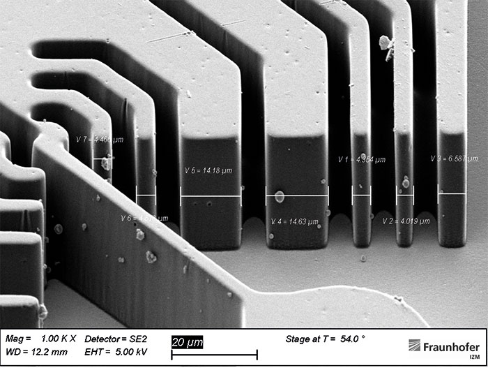
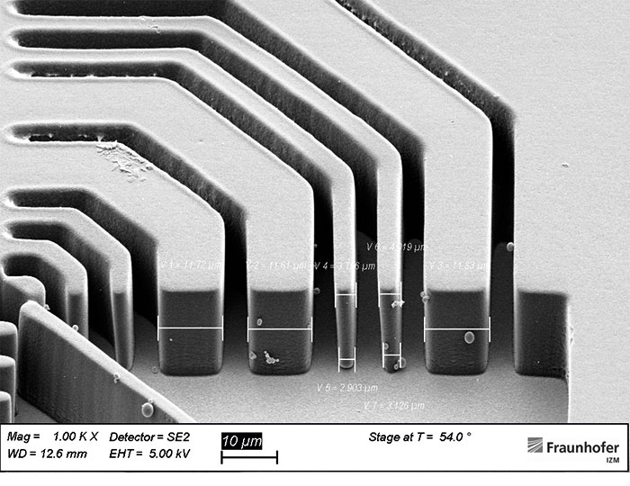
Embedding of high-IO naked chips in IC substrates
Project CHARM ECSEL JU
Contribution of Fraunhofer IZM:
Adaptive Panel Layout (APL), based on precise AOI measurement and multicore-optimized software for rewiring each panel
SAP-based assembly, RDL with 5 µm L/S on ABF GXT62
Specifications:
Die: 26 mm x 18 mm x 0.180 mm
9197 copper pillars: 20 µm high, 30 µm and 60 µm in diameter
Panel: 610 mm x 457 mm
Responsible for the use case:
Sandvik Mining and Construction Oy
Project partners:
AT&S, Beneq, Besi AT, Besi NL, E+E, IMEC, InnoSent, ITE, IUNET, LGE, LUAS, MCL, PacTech, Qplox, Quantavis, RTU, SAF Tehnika, SSH, Tampere University, and TU Chemnitz.
The project received funding from the ECSEL Joint Undertaking under grant agreement No 876362. ECSEL is supported by the European Union Horizon 2020 innovation program and Austria, Belgium, the Czech Republic, Finland, Germany, Italy, Latvia, the Netherlands, Poland, and Switzerland.
Project website
»At the end of 2024, we launched the ‘Glass Panel Technology Group’,« explains Kahle, highlighting the opportunities for collaboration between Fraunhofer IZM and industry. »With this initiative, we want to develop glass-based substrates for advanced packaging and promote their use in data center technology and high-performance computing. Companies along the entire value chain of glass substrates are invited to join our initiative and join us in advancing glass panel technology.«
Due to its special properties, glass offers a promising basis for technological innovations in microelectronics. In particular, its high dimensional stability enables the production of fine conductor tracks with line widths of less than 5 μm.


Add comment