The backbone of our digital world is made of glass: A network of optical fibers spans the globe and lets data criss-cross our globe. We also experience the digital world through a pane of glass: We interact with the online world every day through the glass display of our smartphones.
For almost 20 years, Fraunhofer IZM has been working on giving glass an even greater role in data transmission. But even today, copper cables are used when data has to be transmitted over short distances in the centimeter range, for example on printed circuit boards.
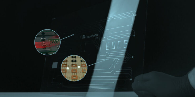
In order to use optical signals for these short distances just as they are used in longer-distance fiber optic cables, IZM invented the electrical optical circuit board (EOCB). And in close cooperation with research and industry partners, a complete process was developed to manufacture EOCBs from glass.
RealIZM has met Julian Schwietering to speak about the fascinating material that is glass, the advantages of electro-optical circuit boards, and the future applications for this photonic assembly technology.
The idea of integrating an optical layer into printed circuit boards was first published by Fraunhofer IZM scientists in 1999. In 2003, it was decided to use glass as the material for the optical layer. The waveguides for this optical layer are fitted in the glass with an ion exchange process, a process that has been known since the 1970s, but was only used on small-format glass.
A team at IZM transferred the technology to large-format thin glass to make it usable for printed circuit boards. To date, IZM is a leader in the production of electrical-optical circuit boards on formats up to 457 mm x 303 mm.
How are optical waveguides integrated into glass? What are the individual process steps involved?
Julian Schwietering, head of the EOCB team in the Optical Interconnection Technologies group at Fraunhofer IZM, knows the answers: “You need quite a long process chain to integrate optical waveguides into glass. This is the process that was developed by us for commercial, mostly closed systems in cleanrooms. Getting people to know about this process is a major concern for me, which is why we created a short film on the subject.”
Electro-optical circuit boards enjoy all the benefits that optical signals have over electrical transmission. In addition, glass-based EOCBs also have all the advantages of glass as a material: very good dielectric properties – especially for high-frequency applications – as well as great dimensional stability, biocompatibility, and high chemical resistance.
For Schwietering, it all starts with the very basics: “Glass is one of the oldest materials known to mankind. Although it has been used in various forms for thousands of years, many effects in glass are still not fully understood. This makes it an exciting material to work with for us researchers.”
Glass: Solid and flexible at the same time
Unlike crystals, glass has no long-range periodicity in its atomic structure. Thanks to the periodic atom structure of a crystal, you can be sure that its fundamental structures (lattice cell) will be the same even after millions of atoms. This makes crystals more predictable. Glass, on the other hand, is amorphous: Its structure consists of three-dimensional connected rings of different sizes, which are arranged unevenly. Many theories from solid-state physics therefore do not work for glass.
Much research is still needed on the fundamental properties of glass, Schwietering admits: “At this year’s conference marking the 100th anniversary of the German Glass Technology Society, a leading glass researcher concluded that the solution to the current challenges in the theory behind the chemical hardening of glass will lie in artificial intelligence. The conventional research methods used so far have not helped us make sufficient progress. There is still much to discover, and glass has incredible potential!” It is no surprise that the UN declared 2022 the International Year of Glass. A leading manufacturer of specialty glass even declared our current times the Glass Age.
The glass future: Larger, thinner and bendable
In the production of EOCBs, the IZM research group uses commercially available borosilicate glass in half-format sizes. This corresponds roughly to the size of a DIN A3 sheet and has a thickness of 550µm. Borosilicate glass is inexpensive and, unlike expensive specialty glasses, readily available in large formats.
“Fraunhofer IZM is, as of now, the only research institute in the world that can functionalize such large-format glass electrically and optically,” Julian Schwietering says. From laminating additional electrical layers onto the glass to processing the glass itself, the researchers* have extensive process knowledge for manufacturing printed circuit boards from glass. “Our goal is to double the size to the so-called full format and, at the same time, make it even thinner to produce flexible EOCBs.”
Common sizes of glass substrates:
– In progress: 515 mm x 510 mm
– Current development status: 457 mm x 303 mm
– Current standard size: 303 mm x 227 mm
“The integration of waveguides now works in a processing-ready manner. This technology could be transferred to industrial use at any time.” Nevertheless, the research work is far from complete. Work is currently underway to integrate additional functions in glass. “We are in the midst of implementing multi-mode interference couplers with our process that split light from a single to multiple waveguides. Furthermore, we are working to automate characterization methods and the permanent coupling to optical fibers. We have already developed an automated measurement station to determine the insertion loss of hundreds of waveguides on one panel. Such equipment is essential if the technology is to be used in industry,” Schwietering explains.
The technology of the future for data centers, (autonomous) e-vehicles, and quantum technology
Electro-optical printed circuit boards are not yet used in commercial production. In addition to telecommunications, the first potential applications for the photonic packaging technology are sensors and quantum packaging.
“We expect EOCBs to be used first in data centers or wherever there is an extremely large amount of data to be processed securely in a very short period of time,” the scientist estimates. It will be a while before EOCBs are also required in consumer products. However, it is only a matter of time before electrical signal transmission will reach its limits there as well.
In addition to the higher data rates, there are other advantages that speak in favor of its use in certain applications. Optical signal transmission is playing an increasingly important role in e-cars when compared to conventional cars with combustion engines. Modern vehicles are increasingly resembling supercomputers. In a battery-powered car, it is important that the individual components, the control elements, and all safety-relevant components are galvanically, i.e. electrically isolated from the battery and the battery management system. In the event of an accident or damage, the safety systems must not be affected by electrical short circuits. The use of optical fibers or waveguides in glass, which do not conduct any electricity, has safety advantages in this respect.
IZM scientists are currently building a QuantumPackagingLab at the Berlin site, which is funded by the European Union and the state of Berlin to the tune of 3.39 million euros. The lab will develop new quantum technologies based on glass. Using highly specialized equipment, the researchers will be able to e.g. produce hermetic packages made from glass and to functionalize them electrically and optically. Laser structuring of glass will also advance, and the coating of glass with nanometer-precise layer thicknesses will become possible at IZM.
Did you know:
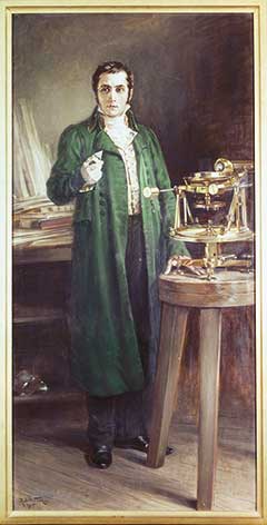
Joseph von Fraunhofer (1787-1826), who gave his name to the Fraunhofer-Gesellschaft, completed an apprenticeship as a glass cutter. He worked as an optician at the “Mathematical-Mechanical Institute” in Benediktbeuren. Within a few years, he was responsible for glass production and the management of the institute. Among other things, he researched the refractive power of glass and the diffraction of light, discovering the spectral lines of sunlight, the “Fraunhofer lines” named after him.
Write a comment so that other readers can benefit from your experience!
Image and Video: Fraunhofer IZM
Image: Joseph von Fraunhofer, Deutsches Museum
Updated at December 4, 2024.