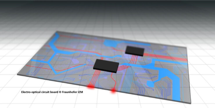
It’s an understatement to say that a lot has changed in microelectronics in the last fifty years – and the same goes for circuit boards. But even greater changes are afoot: with ever more data being used and shared, electrical routing will be complemented more and more by optical conductors. May we present: the electro-optical circuit board made of glass.
RealIZM meets Julian Schwietering from the Optical Interconnection Technologies research group at Fraunhofer IZM to speak about his work on this technology.
What can you tell us about your research?
Julian Schwietering: My research is focused on electro-optical circuit boards, which are circuit boards with both optical and electrical layers. Our approach is unique in that we’re using low-cost commercial thin glass in large sizes of up to 440 mm x 330 mm as the basis of these circuit boards. They have optical waveguides inside the glass, sandwiched between two surfaces with electrical circuits.
Speaking generally, what is the advantage of using electro-optical circuit boards?
Julian Schwietering: The main reasoning behind this research is the same as it was back when we switched internet communication from copper phone lines to fiber-optic cables. Higher data rates were what we wanted, and fiber-optic cables offer higher bandwidths with less signal loss. That’s also why the transatlantic cables have long been fiber-optic cables.
Nowadays, fiber-optic cables go right up to the distribution boxes in the street, and more and more often even directly onto people’s premises. A lot of fiber-optic cables are also used in data centers. Optical connection technology, that is, the transmission of signals by photons, instead of electrons, will become increasingly attractive even for short distances.
One example of this is autonomous driving. For a car to be able to drive completely autonomously, large amounts of data has to be transmitted and communicated. This is pushing conventional electrical circuit boards to their limits, and we will only be able to go further with optical signals.
What sets your research apart from others?
Julian Schwietering: Fraunhofer IZM has done pioneering work in this field ever since the electro-optical circuit board was first invented by us in 1995. We’ve continued to make progress over the last 25 years, and now we’re able to integrate single-mode waveguides in large-sized commercial glass boards using an ion-exchange technique.
That technique itself is well known and used by several research groups and companies all over the world. However, we are the only ones to develop a process to fabricate commercial thin glass up to sizes of 440 mm x 330 mm. This is important to enable large-size circuit boards, or indeed greater numbers of small glass plates in one go, which gets the unit costs down.
We’re staying close to our partners in industry while developing this process, which is typical for a Fraunhofer research group. It’s important for us to use commercial processing equipment. We have now adapted all process steps, except for the ion-exchange furnace, to commercial equipment that can process glass up to sizes of 610 mm to 610 mm. The ion-exchange furnace alone remains as a proprietary development, which allows us to quickly adapt the process, but limits the maximum size to 440mm x 330mm. But we’re working on scaling that up right now.
Using commercially available equipment means that we can eventually transfer that process over seamlessly to our industrial partners, while keeping it very stable.
In general, glass-integrated waveguides in circuit boards are not yet all that common. Some research groups and companies are using polymers to build that optical layer. That works really well for some applications, but we have much that speaks in favor of glass being the best choice for electro-optical circuit boards: There’s the great connectivity you get with glass fibers, their lasting stability, and, more practically, the enormous progress the science has made in glass technology as a result of the demand for stronger glass for our mobile device displays.
What does the production process look like?
Julian Schwietering: The manufacturing process is really many separate processes working together: The glass is first cut into a manageable size and then covered with a metal layer. That metal layer is then coated with a photoresist. After the photoresist has been deposited, a laser direct imaging system writes the required structures into the photoresist, which is then developed and the metal is etched through the resulting openings.
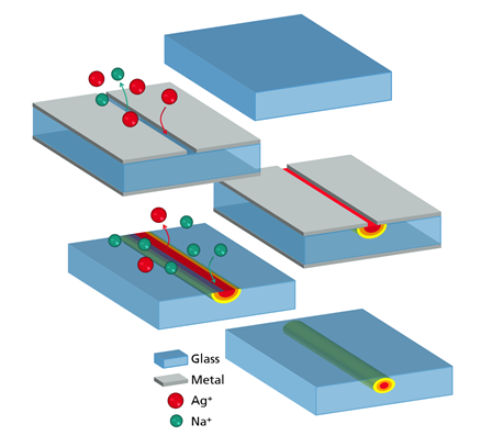
Afterwards the photoresist is removed, and the entire glass panel is put into a molten salt, containing silver ions, where an ion-exchange happens between the sodium ions in the glass and the silver ions from the molten salt. Those silver ions create a higher refractive index in the glass. A second reverse ion-exchange follows next to bury the waveguides into the glass. Finally, a CO2 laser is used to cut the glass into the finished boards. The CO2 laser guarantees the optical facet quality we need, so no polishing is required at the end.
You mentioned that polymers are currently the popular choice for electro-optical circuit boards. Why is that, and why might glass be better?
Julian Schwietering: Polymer is still cheaper to process. Nevertheless, we believe that glass is the better material for optical transmission to a circuit board. Compared to conventional polymer waveguides, it is easier to couple them to a glass fiber because of their similar refractive indices. In addition, there is less attenuation, especially in the 1550 nanometer wavelength range, which plays an important role in telecommunications.
Glass also offers several advantages outside of telecommunications. Glass-integrated waveguides are very promising for sensor applications because of the positive biological properties and high chemical resistance.
What major challenges have you had to master in your research, and what other obstacles can you expect around the corner?
Julian Schwietering: So far, the biggest challenges were to get the manufacturing process safe and stable, and to minimize attenuation. In the wavelength range of 1550 nanometers, we were able to achieve a minimum propagation loss of 0.06 dB per cm, with high homogeneity across the panel.
One issue we’re pursuing currently is the reduction of propagation losses in the curved sections of the waveguides. Achieving smaller bend radii allows higher integration density of the optical circuits.
Future challenges will include the development of connector concepts. Circuit boards should be connectable both at the edges and on the surface of the glass. We have different approaches under evaluation that could achieve the coupling for a wide range of wavelengths with low coupling losses.
What’s in store next? And who are your partners?
Julian Schwietering: We will present the results from our curved waveguides and a novel coupling concept at ECTC at the end of May, probably in a virtual conference. Process development will continue in different research projects, working with our partners at research institutes, universities, and in the industry. Working on molten salts, machine development, optical waveguides, electrical connections, connectors, structuring of glass and much more on top of that means that you need a wide range of project partners, people who are specialized in glass manufacturing, machine development, circuit board producing, placing components, and so on.
Regarding our next steps, we’re working on new concepts to bring the silver ions into the glass, and we’re exploring new applications. There’s research happening in sensor and quantum applications. We are sure, that we can expect a lot from future research, and are happy to work on this fascinating research topic.


Like!! Thank you for publishing this awesome article.