Whether in smartphones, high-performance data centers for AI applications, or automotive electronics – nothing works without assembly and interconnection technology. Electronic packaging protects electronic components and sensors from environmental influences, ensures their functionality even under extreme conditions, enables maximum power densities in the smallest of spaces, and thus contributes to reliability and safety in all areas of application.
Prof. Dr. Ulrike Ganesh, Managing Director of Fraunhofer IZM, talks to RealIZM about current trends and challenges in electronic packaging.
What do you see as the greatest technological challenge?
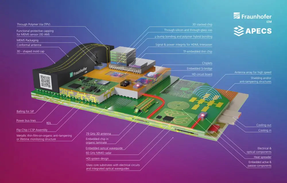
Prof. Dr. Ulrike Ganesh: Historically, the integration density of semiconductor devices has grown rapidly, but this growth is slowing down. We are reaching physical limits, while the demands for performance, energy efficiency, and reliability continue to rise. The purely exponential growth predicted by Moore’s Law has reached its limits. Nevertheless, innovations are advancing in other directions, particularly toward 3D and 2.5D architectures and new packaging concepts that integrate processing, testing, and packaging.
What does this technological trend mean for the development of complex hardware systems?
Prof. Dr. Ulrike Ganesh: As front-end and back-end manufacturing grow closer together, packaging-driven concepts, such as chiplet architectures and 2.5D and 3D integration, are becoming more important. Fraunhofer IZM is working to optimize these approaches and develop practical solutions that combine scalability, power density, and reliability.
How market-ready is 3D integration in semiconductor production today?
Prof. Dr. Ulrike Ganesh: 3D stacking is a key research topic. However, the feasibility of error-free, large-scale production of complex 3D systems still requires valid demonstrations as well as suitable testing and inspection infrastructures. While initial test structures exist, market-ready, widely applicable 3D packaging mass production requires further developments in processing, testing, and qualification.
How important are alternative packaging approaches on the technology roadmap?
Prof. Dr. Ulrike Ganesh: Beyond 3D stacking, we are working on 2.5D integration as well as wafer- and panel-level packaging. Creative combinations of established processes with innovative approaches are opening up new fields of application. One current focus is co-packaged optics using photonic wire bonding.
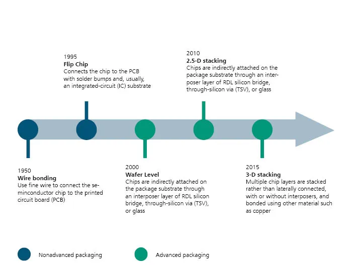
History of connection technology (excerpt)
Sources: Burkacky, O., Advanced Chip Packaging: How Manufacturers can play to win, May 2023, McKinsey Report
What market trends are you currently observing in the semiconductor industry?
Prof. Dr. Ulrike Ganesh: The market structure is shifting. Front-end manufacturers are increasingly integrating packaging solutions into their portfolios. The distinction between chip manufacturing (front end) and packaging (back end) is blurring, leading to new forms of cooperation and value creation.
What role does Fraunhofer IZM play in the interaction between chip development (front end) and packaging (back end)?
Prof. Dr. Ulrike Ganesh: Fraunhofer IZM does not manufacture chips. We develop highly application-oriented electronic packaging solutions for high-tech semiconductor devices that are not yet available in series production. Together with industry partners, we are working on advanced packaging technologies for high-performance computing modules based on advanced node architectures. System Technology Co-Optimization (STCO) emphasizes the need for a holistic view of front-end and back-end aspects. You can expect this holistic view from us.
How will the further development of the research infrastructure be ensured?
Prof. Dr. Ulrike Ganesh: The APECS pilot line enables the state-of-the-art expansion of our infrastructure. The new equipment supports the requirements of the coming years and allows the realization of packaging structures in the submicrometer range. Specific machines promote targeted developments in the fields of photonics, quantum and neuromorphic computing, power electronics, and high frequency. While it is not possible to fully equip all working groups, cross-departmental and cross-institutional collaboration creates valuable synergies.
What is Fraunhofer IZM’s role within the APECS pilot line?
Prof. Dr. Ulrike Ganesh: As part of the Fraunhofer-Gesellschaft and the Research Factory Microelectronics Germany, we work closely with five European pilot lines to swiftly identify suitable partners for cooperation. Within the APECS pilot line, Fraunhofer IZM is responsible for electronic packaging and plays a key role in shaping the future technology roadmap. In Germany, twelve Fraunhofer Institutes and two Leibniz Institutes are involved in the APECS pilot line. Together, we pool our expertise and create tangible added value for the European microelectronics industry.
How important are sustainability and energy efficiency in electronic packaging?
Prof. Dr. Ulrike Ganesh: For over 30 years, our Institute has been developing electronic solutions that use energy efficiently, facilitate recycling, and conserve raw materials. Our employees contribute to making technologies environmentally friendly and reliable. With the support of AI, we can drive forward sustainable electronic solutions even more effectively.
What role does advanced packaging play in the automotive industry, which is so important for Germany?
Prof. Dr. Ulrike Ganesh: The automotive industry is moving toward electrification. Our packaging solutions for the automotive industry help to ensure that electric drives and power electronics remain robust and durable. In this way, we ensure technical reliability while also supporting structural change, jobs, and skill development in Germany.
What application areas is Fraunhofer IZM currently developing for?
Prof. Dr. Ulrike Ganesh: Electronic packaging is a broad field of innovation. We cover the entire process chain for semiconductor components and support companies regardless of their specific process. Our teams conduct research in photonics, quantum computing, aerospace, artificial intelligence, power electronics, and high-frequency technology, among other areas.
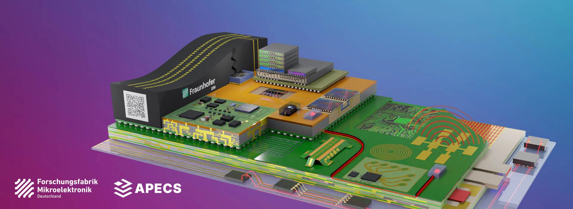
Heterogeneous integration: High-end performance packaging from wafer to system | © Fraunhofer IZM | Mike Groß
How do you see Fraunhofer IZM’s long-term strategic orientation?
Prof. Dr. Ulrike Ganesh: In the medium to long term, we will examine whether to continue our broad expertise or focus specifically on promising technologies. The tension between versatility and specialization requires a balance. At our Berlin site, we work with a wide range of materials and formats, developing prototypes and small series. The Fraunhofer IZM-ASSID site in Dresden is highly specialized in standardized processes with a 200/300 mm 3D wafer-level process line and is geared toward larger production volumes.
Thank you very much for talking to us!


Add comment