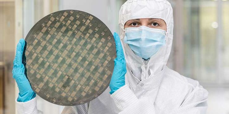
For more than 10 years, the “All Silicon System Integration Dresden – ASSID” center has been operating a state-of-the-art, industry-grade 200/300mm 3D wafer-level process line with modules for TSV formation, pre-assembly (thinning, separation), wafer-level assembly, and stack formation. The ASSID is part of Fraunhofer IZM, and its philosophy is to deliver test samples to its customers in less than a year.
Dr. Manuela Junghähnel has been in charge of the Dresden-Moritzburg site since 2022. She has many years of experience in the field of wafer-level system integration. In her interview with RealIZM, she talks about which topics will matter tomorrow, which research is happening today, and which core competences for packaging on 300mm wafers will be the focus of her leadership.
What would you consider particularly important for the next ten years of Fraunhofer IZM-ASSID?
Dr. Manuela Junghähnel: At Fraunhofer IZM-ASSID, we consider all current trends and developments in microelectronics highly relevant. Securing Europe’s standing in the field of electronics and increasing domestic chip production, not least when you see Saxony’s place as a hotspot: Those are some of the topics we are actively shaping with our work.
Since the foundation of our institute 12 years ago, a lot has been invested at the site. But in the semiconductor industry, the cycles during which equipment can still be considered up-to-date are significantly shorter than in other industries. This means that we are always feeling the urge to have the right equipment and infrastructure to keep pace with the demand for the latest technologies and newest developments.
I want to put IZM-ASSID in the best possible place for the future – for example, following the trend toward high-density integration, higher precision, new materials, or new areas of application like high-performance or quantum computing. So, it’s all about innovations and technologies for the packaging of the future.
Fraunhofer IZM’s center “All Silicon System Integration Dresden – ASSID” operates a leading-edge, industry-compatible 200/300mm 3D wafer-level process line with modules for TSV formation, pre-assembly (thinning, singulation), wafer-level assembly, and stack formation. ASSID focuses on process development, material and equipment evaluation as well as R&D services and prototyping.
Advanced pilot line for wafer-level packaging:
– 3D Wafer-Level Systems-in-Package
– Copper-through-Silicon Via (TSV) Formation
– Wafer Thinning and Thin Wafer Handling
– Interposers with High-Density Redistribution
– 3D Assembly and Interconnection Technologies
The International Certification Group (ICG) confirmed 2018 that the quality management system of the “Wafer Level System Integration” (WLSI) department is in accordance with the standard DIN EN ISO 9001:2015 and has been officially certified for “Research, development, and services in electronic packaging”.
What strategic goals have you set yourself for the site?
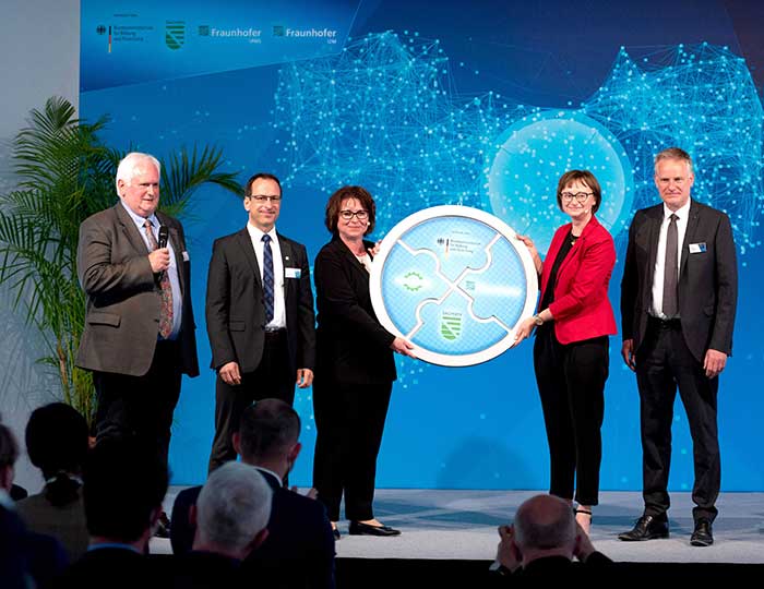
Dr. Manuela Junghähnel: Our future will definitely be one of growth. In June 2022, Dr. Wenke Weinreich, Site Director of Fraunhofer IPMS-CNT and Deputy Director of IPMS, and I opened the new cleanrooms of the Center Nanoelectronic Technologies (CNT) and the 300mm Center for Advanced CMOS & Heterointegration in Dresden-Moritzburg.
With our expansion at the secondary site at Fraunhofer IPMS-CNT, we are starting cross-institute collaboration. We are bringing together competences and seizing synergies related to 300mm wafer technologies to be able to offer our customers a broader portfolio of R&D services*.
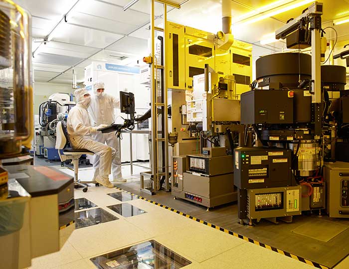
We have 900 square meters of cleanroom space at this site. And we already have a concept in place for investments that we need to keep up with current and future requirements. This is the only way we can offer meaningful R&D services in a pilot line and respond to strategically important topics, such as high-performance or quantum computing, with technology solutions for 300mm wafer-level system integration.
That is how I see Fraunhofer: To develop, test, optimize, and manufacture technologies in small production runs for our industry clients. We will be able to do this better with the expansion of the IZM-ASSID. High-precision bonding tools, but also our lithography and PVD equipment and the means for testing new materials, for example, play an important role here. I see the fact that we are developing packaging technologies on 300mm wafers as a unique selling point of IZM-ASSID, even within Fraunhofer.
The Center Nanoelectronic Technologies (CNT) is a business unit of the Fraunhofer Institute for Photonic Microsystems IPMS.
– Applied research on 300 mm wafers for microchip producers, suppliers, device manufacturers, and R&D partners
– 4,000 m² of class-6 and class-3 cleanroom space (according to ISO 14644-1) and laboratory space for more than 80 processing and analytical tools
– Deposition and etching as well as inspection and analysis equipment for determining defects and measuring layer properties
The opening of the Center for Advanced CMOS & Heterointegration Saxony was a highlight. What is Fraunhofer IZM-ASSID’s part in it, and how can you benefit from it?
Dr. Manuela Junghähnel: The two partners bring different competences to the table: At IZM-ASSID, we are the 300mm specialists in backend processing for wafer system integration, assembly, bonding, 3D integration like TSVs, or the formation of interconnects. But there are also other upstream processes that Fraunhofer IPMS-CNT is highly specialized in, like active devices, energy-efficient or non-volatile memory, and much else. Fraunhofer IZM-ASSID and IPMS-CNT – both are unique R&D actors in the field of microelectronics in Germany.
With our center, we are bundling our R&D activities based on 300mm wafer industry-standard equipment and the competences for frontend and backend technologies as well as wafer-level system integration. It is the entire value chain. The units of both Institutes have already been working together on projects for many years. In that sense, our work at the newly opened Center is not only a natural next step, it is the logical and right step for us.
Thank you for the interview! We are looking forward to much more exciting research from Dresden.
The interview was conducted by Susann Thoma
Images: Silvia Wolf, Fraunhofer IZM-ASSID and Fraunhofer IZM/ Christian Schneider-Broecker
If you liked the article, please share it on LinkedIn, Twitter, Instagram or Facebook. If you have something to say, we welcome your comments.