In the »CeCaS« research project, a consortium led by Infineon Technologies is working on an innovative software design process and hardware for the high-performance computing applications needed for the automotive control modules of the future. This includes work on an efficient method for the automated design of software for autonomous driving.
A key prerequisite for this sophisticated software architecture to work is the creation of reliable hardware for the purpose. As part of the project, the »Assembly and Encapsulation« working group at Fraunhofer IZM was responsible for three different chiplet designs on organic circuit carriers.
Karl-Friedrich Becker, group manager for Assembly & Encapsulation Technologies, and Steve Voges, process development engineer at Fraunhofer IZM, have joined RealIZM to talk about the thermomechanical challenges of chiplet modules for HPC applications and opportunities for optimizing the process.
Chiplets only work in combination. A chiplet is a component that specializes in a specific function. It forms an IP block and has a communication interface for interacting with other chiplets. A single chiplet could not simply be packaged up in its housing and expected to operate independently.
»Our task is to design the packaging interfaces between the chiplets in such a way that fast and highly efficient communication takes place between the individual IP blocks,« says Karl-Friedrich Becker, describing the focus of Fraunhofer IZM’s work in the research project »CeCaS«, which stands for »Central Car Server«.
The research teams of several automobile manufacturers and suppliers are working closely with industry partners and research institutions in various semiconductor technology projects and alliances, such as the »Chiplet Center of Excellence (CCoE)« and the »Automotive Chiplet Program (APC)«. Their mission: Mastering the challenges of high-performance computing applications and reliability requirements and actually creating the chiplet modules themselves at a later stage.
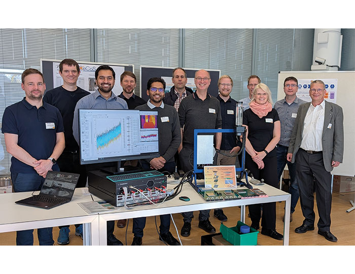
Final meeting of the CeCaS project I © CeCaS
Heterogeneous integration and the research focus of the »CeCaS« project
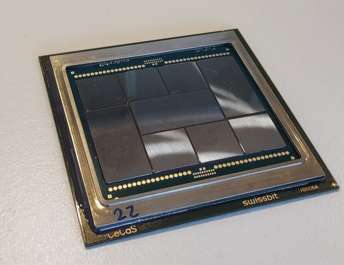
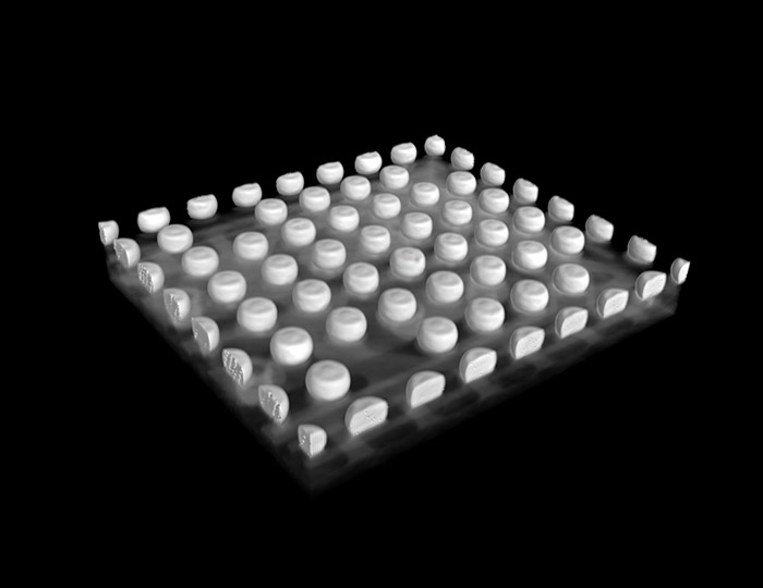
»Heterogeneous integration – packaging different chiplets from different fabs on a single platform – is the core of the research being done at Fraunhofer IZM,« explains Karl-Friedrich Becker. As part of the »CeCaS« project, he and his team have implemented three separate chiplet structures on organic circuit carriers using flip-chip mounting: »We packaged chip sizes ranging from 10 x 10 mm² to 40 x 40 mm² with pitches from 300 µm (TTC) to 150 µm (DC), achieving silicon areas of more than 1900 mm² per package.«
Three test vehicles are used to investigate the questions the researchers are still exploring. With their help, technologies and processes such as flip-chip assembly, underfill, balling, and board assembly have already been improved. In addition, new insights have been gained into heat dissipation strategies and reliability models.
Reliability assessment and test vehicle
The reliability of the thermal test vehicle – with a chip area of 40 x 40 mm² and 300 µm pitch – was assessed by Fraunhofer ENAS based on the manufacturing data and tolerances provided by Fraunhofer IZM. There is both a monolithic design of this vehicle and a design consisting of three chiplets. The vehicle was used to test the design of the overall housing.
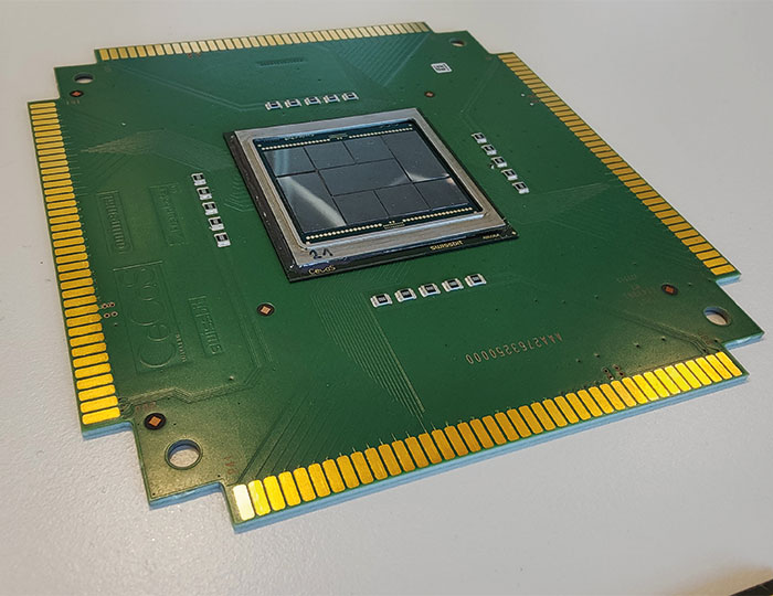
The electrical test board has a silicon area of 40 x 40 mm² and a pitch of 150 µm. The large-area coverage of the thinned chips on the board helps to familiarize users with the manufacturing technology. On the electrical test board, project partner Swissbit implemented a specified design based on netlists. The aim of their design was to connect test structures at the different levels from the chip to interposers to the mainboard in such a way that contact integrity could be verified at every packaging level for the entire structure.
The first assembly tests of this complex 3D structure were conducted at Fraunhofer IZM. Initial inspections and assembly tests were carried out, the assemblies analyzed, and the findings passed back to Swissbit. »With this lab-to-fab approach, we were able to gain important experience with manufacturing chains and the thermo-mechanical challenges that can arise with a large chip area of 1600 mm² and a triple stack – chip, interposer, and carrier substrate,« Becker explains.
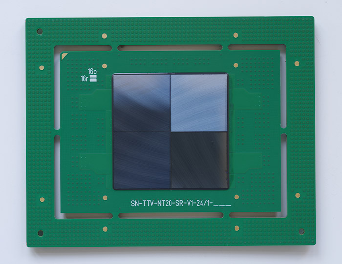
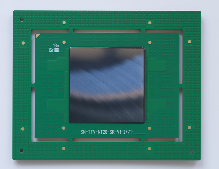
Left: TTV 1 after underfill setup | © CeCaS
Right: TTV 3 after underfill setup | © CeCaS
The third test board, measuring 70 x 70 mm², contains chips of different sizes and in different arrangements, as the layout of the chips is adapted to specific applications. The point here was to investigate how heat conduction can be designed to work best upwards and downwards.
ETV with stiffener and ETV on testboard | © CeCaS
Thermomechanical challenges and solutions in the flip-chip assembly of chiplets
Steve Voges, process engineer at Fraunhofer IZM, cites the handling of large chips as one of the challenges in the project: »The trend over the last ten years has been towards ever smaller and finer chips, with the corresponding size of the connections. Our machines are designed and set up accordingly. Now, chips with very fine structures are becoming larger again.« Karl-Friedrich Becker adds: »We have been working with large flip chips for a long time. As researchers, it is very exciting for us to see the evolution of our work. With the »CeCaS« project, we have taken the next important evolutionary step.«
Voges sees the effect of thermal mismatches during production as the second key challenge: A printed circuit board has a coefficient of expansion of 18 ppm/K, but the chip on the printed circuit board has a coefficient of expansion of 2 ppm/K. In addition, the chip uses normal tin-silver-copper balls. In the reflow oven, the temperature is first raised to 260 degrees Celsius and, after a short holding time at 220 degrees, cooled back down to room temperature. As a result, the solder solidifies at 220 degrees and, as it cools down further, the materials contract against each other – the chip only slightly and the substrate very strongly. This results in mechanical stresses in the module and ultimately in warped modules. »It is our responsibility to optimize the choice of materials and to design the temperature control during this process in such a way that the structure warps only slightly when it cools down and only minimal stresses arise due to contraction.«
Efficient process optimization for automotive packages
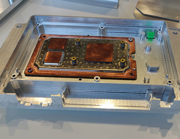
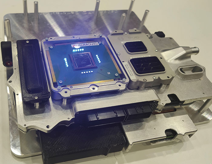
But what exactly is an automotive package? Becker describes it as follows: »Chips are mounted on a substrate. This substrate with the chips is then placed on a carrier substrate. The carrier substrate contains additional electronics, the power supply, and communication interfaces for the sensor technology. This assembled circuit board is then placed in a die-cast aluminum housing. Among other things, this housing contains the electrical contacts (automotive connectors) and the connection for the cooling water. This package – the Central Car Server – can then be installed in a vehicle. At Fraunhofer IZM, we manufacture the core component, which cannot function on its own.«
To achieve this, the researchers used measurement technology to investigate what actually happens when scaling up to larger chip areas in flip-chip assembly. They determined in advance what would happen in order to adapt the measurement technology used previously for smaller structures to larger chip structures and ensure that the processes would still continue to function. The profile of the chiplet structures was also measured precisely in three dimensions after each individual process step to identify any warping. Using an agile process control approach, the scientists were able to adapt the processes very quickly as needed.
Left: TTV 2 on test board in cartridge, ready for installation in the vehicle © CeCaS
Right: ETV on demo module | © CeCaS
Karl-Friedrich Becker explains: »We moved forwards with process optimization in a knowledge-based manner, that is, by using numerous intermediate measurements to evaluate the thermomechanics in the structures very quickly. Despite the limited number of substrates available, we were able to make great progress in a very short amount of time and with only a few trials.«
Becker and his team record a complete data set for each setup. In order to improve the complex process chain, the manufacturing quality data was also correlated with the product quality data. The collection and structuring of process information is an important contribution to the digital twin for reliability assessments.
TTV 1 & 3 3D model bump array | © CeCaS
The experts for reliability assessments for electronics at Fraunhofer IZM link the correlation with analytics to be able to make a statement about how manufacturing affects the model and what the model says about future reliability and product quality. By assessing the condition of electronics during manufacturing, valuable information can be gleaned about the reliability and service life of electronic systems/assemblies.
Rapid integration of new technologies into automotive systems using chiplet technology
»If, for example, you replace only the AI unit in a system that is already qualified in terms of geometry, chip size, and materials, and it comes from the same fab, has a similar bump configuration, and offers greater performance because it has been optimized, then you save a lot of requalification effort,« Becker says about the advantages of chiplets for automotive applications. This makes it possible to introduce the next generation without some of the costly qualification process.
This flexible system approach and the emphasis on reliability are of great importance, as progress and the evolution of the various components – for example, computing units, AI units, or standardized memory units – proceed at different speeds. The chiplet approach makes it possible to leave essential parts of the design unchanged and replace only individual components as needed. This facilitates the integration of new technologies into existing systems. The »CeCaS« project is an impressive demonstration of how research and industry are working together on the future of driving.
CeCaS – Supercomputing platform for highly automated vehicles
CeCaS | The abbreviation »CeCaS« stands for »Central Car Server«. |
Duration | 12/2022 – 11/2025 |
Funding body | ederal Ministry of Research, Technology, and Space (formerly BMBF) |
Funding amount | 46.2 million euros under the MANNHEIM research funding guideline (»Electronics and software development methods for the digitalization of automobility«) |
Funding code | 16ME0800K |
More Information | |
Coordination | Infineon Technologies |
Project partners | Ambrosys, AVL Software & Functions, AUMOVIO, Berliner Nanotest und Design, Bosch, CARIAD – Automotive Software for Volkswagen, emmtrix Technologies, FZI Forschungszentrum Informatik, Fraunhofer ENAS, Fraunhofer IMWS, Fraunhofer IPMS, Fraunhofer IZM, Glück Engineering, Hella, Hochschule München, Inchron, KIT Karlsruher Institut für Technologie, Kernkonzept, Missing Link Electronics, STTech, Steinbeis ZFW, Swissbit Deutschland, Technische Universität Chemnitz, Technische Universität München AIR, LIS, SEC, Universität zu Lübeck, ZF Friedrichshafen |
© CeCaS