The semiconductor industry is increasingly relying on modular chiplet systems to maintain the exponential growth in computing power. Innovative technologies such as 3D heterointegration and electro-optical co-packaging play a central role in this endeavor.
The Fraunhofer Institute for Reliability and Microintegration IZM is actively promoting the development and integration of chiplet technologies as part of the APECS pilot line, which is being set up as part of the EU chip program to promote chiplet innovations and build up more research and production capacity for semiconductors in Europe.
In their interview, Rolf Aschenbrenner and Erik Jung from Fraunhofer IZM and Dr. Michael Töpper from the Research Fab Microelectronics Germany (FMD) speak about how the APECS pilot line helps companies introduce novel technologies in the field of advanced packaging and the integration of chiplets.
Can you please briefly explain in which areas Fraunhofer IZM is working on developing new chiplet technologies?
Rolf Aschenbrenner: At Fraunhofer IZM, our focus is on hardware integration. With our extensive technology kit for hetero-integration, we can produce chiplet modules and support system design, reliability, and testing.
Erik Jung: This is why we see our work from a holistic systemic perspective when it comes to integrating and optimizing chiplet modules. Starting with the unhoused chip still in the wafer stack, we add metallization, for example, or bumps for fine-pitch contacting. We pursue this approach not only for high-performance CMOS chiplets, but also III-V based RF or optoelectronic chiplet components.
You cannot have chiplet systems without heterointegration! In this sense, high-end performance packaging from wafer to system is crucial for new hardware and for the sustainable success of chiplet technology.
Fraunhofer IZM’s technology kit: High-end performance packaging of wafers and systems is essential for creating the APECS pilot line hardware | © Fraunhofer IZM I Mike Groß
How could the APECS pilot line contribute to Germany’ and Europe as places to do business?
Michael Töpper: The evolution of chiplets is currently being driven by large semiconductor companies that can bear the high costs of manufacturing wafers and the necessary sub-7 nm masks. With the APECS pilot line, we offer start-ups and small to medium-sized enterprises (SMEs) that do not have resources like these a hardware platform and open up opportunities for applications that will come onto the market in the next few years.
Rolf Aschenbrenner: The EU Chips Act wants to increase the share of chip production in Europe from the current nine percent to 20 percent by 2030. In order to integrate and functionalize chiplet technologies, special know-how and technologies for assembly, mounting, and substrates as well as access to research infrastructures are crucial.
Which target groups is the APECS pilot line meant for?
Erik Jung: The APECS pilot line is meant for the entire European microelectronics industry, from start-ups and SMEs to large companies, including suppliers to the automotive sector or research institutions. Access is open to all. We offer a complete platform for all suppliers in the value chain, from foundries and Integrated Device Manufacturers (IDM) to Outsourced Semiconductor Assembly and Test (OSAT), microsystems and electronics users, training organizations, universities, testing specialists, and material manufacturers.
Michael Töpper: The APECS pilot line is focused on cooperation with European institutions. However, as the development of microelectronics is transnational, we are also planning cooperation with Japan, Taiwan, South Korea, and the USA.
What added value will the APECS pilot line offer the semiconductor industry?
Erik Jung: With the APECS pilot line, we are creating a bridge between research and industrial practice. The partners on the pilot lines work together to develop technologies that are often too complex, time-consuming, or costly for individual companies on their own. The aim is to enable partners to test and implement modern technologies for new concepts and transfer them to production without major hiccups. This gives companies clear information about which devices they need for specific processes and which framework conditions are crucial for making the optimal selection for their product portfolio.
Michael Töpper: Instead of saying that something is technically impossible or too complex, the APECS pilot line is there to help turn new ideas into reality and open up new markets. We want to give research institutes, start-ups, and SMEs easy access to producing hardware prototypes in small batches of several hundred units. At Fraunhofer IZM, Start-a-Factory is already showing successfully how this works. With APECS, we are taking this approach to the field of high technology.
It’s not just about silicon chips, but also about high-frequency chips based on III-V semiconductors as well as MEMS and optoelectronic components. The entire concept can be extended to other manufacturing technologies in the semiconductor world.
How does the APECS pilot line differ from a normal production line?
Rolf Aschenbrenner: APECS is a state-of-the-art research facility for the development of high-precision integration technologies and modular chiplet architectures. The evolution of high-precision integration technologies (2D, 2.5D, 3D) is essential for us to be able to create highly functional systems.
The prototyping of organic substrates with structures down to one micrometer or new materials such as glass are crucial for applications in artificial intelligence and high-performance computing. There is a considerable need for research in the areas of substrates, assembly, and integration, which APECS will drive forward.
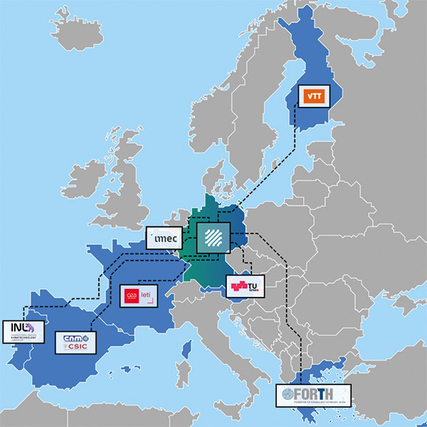
The APECS consortium brings together the technological competences, infrastructure, and know-how of ten partners from eight European countries. | © loewn
How does the APECS pilot line differ from the other European pilot lines?
Rolf Aschenbrenner: APECS works together with the FAMES and NanoIC pilot lines. The consortia of these three pilot lines have set up a number of projects to establish and expand that collaboration.
Erik Jung: By contrast to the WBG pilot line, which is being set up from scratch in Tampere, Finland, the APECS pilot line is based on the already extensive technological portfolio of the twelve participating Fraunhofer Institutes and the two Leibniz Institutes FBH and IHP. By incorporating existing equipment, APECS will also drive forward key innovations there and work to join forces with the other pilot lines.
Where will the APECS pilot line be located?
Rolf Aschenbrenner: The research infrastructure will be distributed decentrally across various Fraunhofer Society sites. A Manufacturing Execution System (MES) will ensure the complete throughput and transportation of chips and wafers between the participating facilities.
What is the advantage of spreading a pilot line across different locations?
Michael Töpper: One major advantage is the ability to use different materials, as not all of them, such as gold, can be processed in a clean room. In addition, every Fraunhofer Institute and every Leibniz Institute is closely linked to one or more university institutions, which contributes to even more significant scientific impetus for research, as local expertise can be brought in.
And how will Fraunhofer IZM be involved in the pilot line?
Rolf Aschenbrenner: Fraunhofer IZM will be involved in the pilot line at the two sites in Dresden and Berlin. In Dresden, Fraunhofer IZM-ASSID and Fraunhofer IPMS are part of the APECS pilot line, both as 300 mm sites. The Saxony-based institutes Fraunhofer ENAS and Fraunhofer IIS-EAS are also on board.
Erik Jung: It should not be underestimated that the Berlin region is also benefitting from around 50 million euros in support for new infrastructure, which can be seamlessly integrated into the existing expertise in the region. With the APECS pilot line, we will provide a new quality and quantity to promote the European microelectronics industry.
Rolf Aschenbrenner: At Fraunhofer IZM in Berlin and Fraunhofer IZM-ASSID in Dresden, we are creating infrastructure for interposer technologies – be it silicon, organics, or glass on 200 mm wafers or 300 mm wafers and panels on organics. An offering in this form and variety is unique worldwide. With the newly founded Chiplet Center of Excellence (CCoE) in Dresden, we want to set new standards for automotive electronics together with Fraunhofer IIS/EAS and Fraunhofer ENAS.

From left to right:
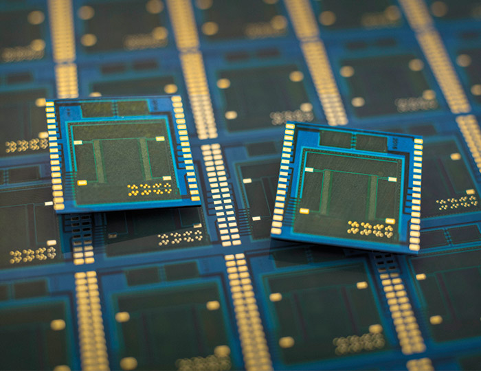
Multi-Chip Stack with Microbumps as Connection Elements | © Fraunhofer IZM I Volker Mai
Advanced Fan-Out Wafer and Panel Packaging based on Embedded Technologies | © Fraunhofer IZM I Volker Mai
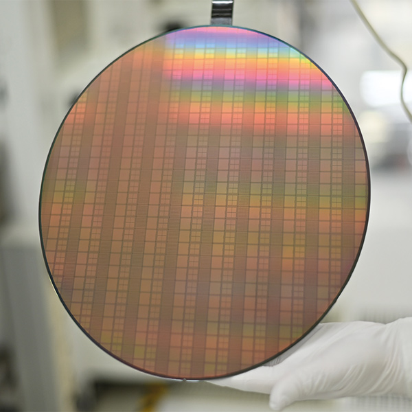
Demonstrator: 300 mm Si-Wafer with High-Density Copper Connections for Chiplet Integration within the “T4T” Project Copyright | © Fraunhofer IZM-ASSID, Silvia Wolf
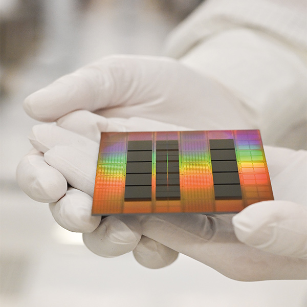
Demonstrator: Assembled Chiplets with Ultra-Fine Copper Hybrid Bond Contacts on a Pitch of 10 µm | © Fraunhofer IZM-ASSID, Silvia Wolf
Which industries is this kind of technical infrastructure important for?
Rolf Aschenbrenner: The potential applications for chiplets are very diverse: wherever extremely high computing power and very high integration density are required, e.g. for AI applications in the automotive and industrial electronics sectors.
Erik Jung: In addition to high-performance computing (HPC) and AI clusters, application scenarios are also conceivable in which data processing takes place directly on the sensor node (edge AI) – i.e. directly at the point of data collection – with the support of artificial intelligence. In industrial electronics, complex image processing could conceivably take place directly on the sensor node. Highly integrated chiplets in an optimized combination of computing, energy supply, and wireless technologies could become a game changer here.
Michael Töpper: At the Consumer Electronics Show (CES) in Las Vegas at the beginning of the year, televisions offering AI-supported automatic translations were presented for the first time. Artificial intelligence will create new applications in all industries. In mechanical engineering, for example, AI combined with object recognition will create extraordinary opportunities.
When will the APECS pilot line be operational?
Michael Töpper: There are already opportunities for cooperation that will be taken to a higher level of technology as part of the expansion. We have already received the first inquiries.
What opportunities for cooperation does the pilot line offer for players in Germany and Europe?
Rolf Aschenbrenner: The entry points for cooperation with the APECS pilot line can be diverse. The APECS pilot line fundamentally supports the development of a holistic system design and conveys an understanding of the process. This includes the definition of chiplet interfaces and the production of substrates as well as reliability tests and the production of a complete chiplet module.
Usually, companies already have a plan to implement a chiplet module, but need support with developing an organic interposer. In this case, the entry point would be a project with us at Fraunhofer IZM in the APECS pilot line to create an organic interposer for chiplets and produce a functional chiplet module.
Erik Jung: Companies could also get training in state-of-the-art processes, pay for contract research, or carry out exclusive pilot production runs. The APECS pilot line offers European partners customized access models and solutions for such scenarios.
Michael Töpper: I would like to emphasize that the connection to chip design is important to us. We are not only focusing on the technology but are also pursuing the System Technology Co-Optimization (STCO) approach with APECS. It is important to us to bring chip design closely together with technology in order to create feasible solutions and at the same time open up new possibilities for chip designers.
What role does the office of the Research Fab Microelectronics Germany (FMD) play in setting up the APECS pilot line?
Michael Töpper: The FMD office has many purposes: we are responsible for the entire project management and marketing, coordinate the purchase of equipment, and manage the development of the demonstrators. We are also the central interface for the project sponsors on the German and European level and act as a matchmaker for European semiconductor technology.
You just mentioned the development of demonstrators. What exactly are you planning?
Michael Töpper: To demonstrate the functionality of the APECS pilot line, four demonstrators are being developed that cover different areas of the technological portfolio: High-frequency technology, opto-electronics, high-performance computing, and the integration of MEMS technology.
Who could interested parties contact, and how should they do that?
Michael Töpper: Our team of experts is on site in Berlin and can also be contacted at any time by email at experts@mikroelektronik.fraunhofer.de. We put interested parties in touch with the relevant contact person from our network very quickly. It is important to us to answer inquiries in a service-minded manner. If necessary, we also provide support. However, our partners, such as Fraunhofer IZM, are responsible for preparing offers and providing the service.
Do interested parties have to observe certain criteria when making initial contact, e.g. send a pitch deck?
Michael Töpper: There is no formal process or ready-made solutions; the key lies in the conversation. In discussions with our experts, it often becomes clearer to customers what they really need and which additional aspects, such as chip design, they need to consider. With our consulting services, we offer customized solutions.
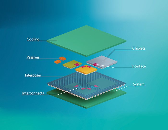
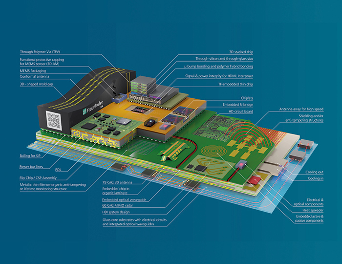
Simplified representation of chiplet design © Fraunhofer IIS
As Erik Jung has already mentioned, we can often help a lot with smaller activities such as training courses. One example could be a three-hour workshop in which experts explain what exactly is meant by the term »chiplet«.
What milestones are on the FMD office’s agenda for 2025?
Michael Töpper: Our core task for 2025 is to make the services offered by the APECS pilot line visible and to set up the management structure. This year, we will be presenting the pilot line at selected conferences and trade fairs such as Sensor+Test in Nuremberg, EuMW in Utrecht and SEMICON EUROPE in Munich.
Another important goal is to intensify the exchange with the partners already involved in the consortium and the project. Together we form the APECS pilot line and our task is to get it up and running.
Thank you very much for the interview!
Coordination | Fraunhofer Society |
Implementation | Research Fab Microelectronics Germany (FMD) |
Project partners (national) | Twelve institutes of the Fraunhofer Group for Microelectronics and two Leibniz institutes FBH and IHP |
Project partners (European) | TU Graz, VTT, imec, CEA-Leti, FORTH, IMB-CNM-CSIC, INL |
Duration | 11/1/2024 to 06/30/2029 |
Funding | The project was funded as part of the APECS pilot line by Chips Joint Undertaking (which is funded by Horizon Europe and the Digital Europe Program) and co-financed by national funding from Austria, Belgium, Finland, France, Germany, Greece, Portugal, and Spain. |
More information |