RealIZM blog series »Microelectronic Trends« – Part 1
Why is heterogenous integration considered a game changer for the next generation of semiconductor technology? In his interview with RealIZM, Erik Jung, Business Unit Developer at Fraunhofer IZM, gives an insight into the challenges faced by semiconductor manufacturers and research institutes trying to develop and make electronic components and systems with maximum performance.
Heterogeneous integration: What does the term actually mean?
Erik Jung: In heterogeneous integration, or hetero-integration for short, semiconductor components from different domains, e.g. optical, mechanical, or CMOS components, are combined – each from their optimized type of production – to achieve maximum performance. When we integrate them, we make sure that the paths between the individual functional units are kept so short that the signal latencies are as low as possible.
In the past, semiconductor components with different functions were often processed in a single – monolithic – production line. For example, high-frequency switches were integrated on a CMOS platform. Although this may be cost-effective, it is not optimal in terms of functionality or performance. This approach, called the system-on-chip (SoC), was promoted particularly in the field of cell phones. But it only really makes sense if the components’ performance and environmental requirements can be realized on a production line and the compromises that need to be made have no major impact on the system’s function. However, this case is becoming increasingly rare.
For higher-intensity transmissions, for example, more power must be dissipated via the system’s high-frequency section. This requires a different type of cooling. Power must also be supplied in a different way, for example from the rear. However, you cannot do this anymore with CMOS-based technology like a system-on-chip (SoC).
Is there a difference between the terms hetero-integration and hetero system integration?
Erik Jung: The difference lies in how much gets integrated. In hetero-integration, semiconductor components from different processes are combined, e.g. a component from CMOS production with a VMOS semiconductor for power control. In hetero system integration, it is not enough to simply combine components; the entire system’s functionality is included.
How long has hetero-integration been around?
Erik Jung: The term hetero-integration has been around for a long time, but it started to receive greater attention around 20 years ago. Philips made it clear to the public that the so-called “Moore’s Law” would eventually reach its physical limits and that we needed a new paradigm: “More than Moore” would enable significant improvements in the performance of systems.
In 1965, Gordon Moore came up with the rule that the number of transistors on a chip, and with them its computing power, doubles approximately every two years.¹ There are now 100 billion transistors on the most modern semiconductors.
Thanks to constant advances in production technology, the tipping point has been postponed time and again. But now it is highly likely that we will reach this point in around three to five years. The current performance parameters of supercomputers are a good indicator of this. It is no longer enough to increase the chip area used in order to up the computing power, storage space, or sensor capabilities in supercomputers. This can only be achieved by increasing the number of chips. This is why the topic of hetero-integration is increasingly coming to the fore.
To enable even more communication in an SoC or a CMOS system, we need a method that goes beyond Moore’s prediction: “More than Moore”. In an adjunct to his famous rule, the engineer Gordon Moore already pointed out that it can prove more economical to build large systems from smaller functions that are manufactured separately and ultimately interconnected. So the man who gave the rule its name was himself already thinking further ahead than generations of semiconductor engineers after him. For us, this means that we now have to focus more on heterogeneous integration.
In your opinion, which types of application will benefit most from heterogeneous integration?
Erik Jung: From a global economic perspective, hetero-integration plays a role everywhere: in high-performance computing, in medical technology, in mobility, in renewable energies, and in smart farming. Hetero-integration is used in very different ways in all of these areas. Depending on the area of application, specific processes are used, and quite different cost targets are pursued.
It is important to understand that a sensor application for use in the “Internet of Things” is approached differently in terms of its components than an automotive system for autonomous driving or a high-performance computing system used for training large language models with the help of artificial intelligence.
What technological processes are available for hetero-integration?
Erik Jung: Hetero-integration is best thought of as a powerful technology toolbox. Similar to a Swiss army knife, various excellent tools – in our case technological processes – are available. The appropriate technology set is selected depending on the application. We start by working out, in preliminary studies, which processes are best suited to the application, e.g. fan-out packaging or quasi-monolithic integration.
In order to make the right choice, the challenges of each use case must be taken into account and the question of added value for customers and users must be answered. For some applications, it is already clear which tool sets are suitable for which components. For other applications, we are still in the discovery phase.
The cover of the Fraunhofer IZM brochure shows the institute’s technology portfolio in high-end performance packaging. To what extent does this image represent hetero-integration?
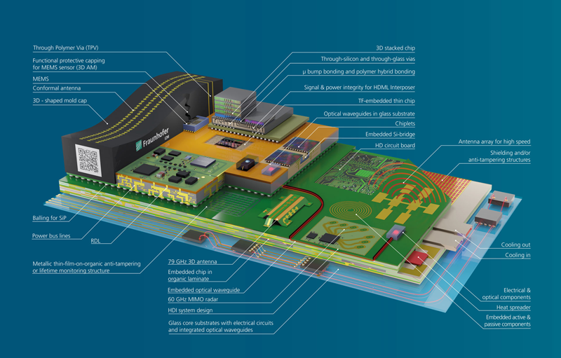
Vision of hetero-integration using the example of high-end performance packaging, | © Fraunhofer IZM
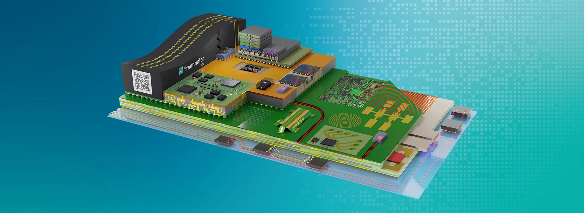
Erik Jung: The graphic shows our vision for hetero-integration using the example of high-end performance packaging. It presents the technology toolbox that is available for hetero-integration here at our institute. When creating this image, we asked all department and group heads which topics they believe constitute heterogeneous integration.
As a result, we can see that heterogeneous integration is an incredibly powerful method for building a system in miniaturized form using a variety of approaches. Heterogeneous integration encompasses a large technology portfolio across the various package levels. Everything has shifted closer to the chip compared to 30 years ago:
- Level 0 is the chip,
- Level 1 is the integration of chips on a wafer or the stacking of chips on top of each other,
- Level 2 is the integration layer with organic interposers or glass interposers with the connections for the subsequent system components,
- Level 3 is the substrate as a system carrier with added functionality.
We would not offer our customers the type of toolbox shown in the picture. That would be a one-size-fits-all solution. When we work on behalf of our customers, we analyze which technologies are suitable and expedient for the specific application, e.g. 3D stack integration, PCB integration, or glass interposer integration.
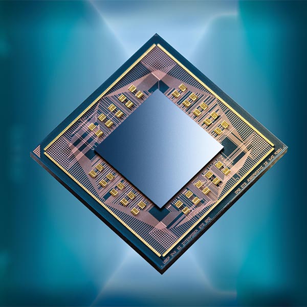
Left: Example of Level 1 integration: Trial interposer for testing the design and functionality of the USeP project’s Risc-V processor made with the 22FDX® technology | © Fraunhofer IZM I Volker Mai
Center: Example of Level 1 integration | © Fraunhofer IZM I Volker Mai
Right: Glass interposer: Hermetically sealed glass package for HF applications with TGVs & integrated ASIC | © Fraunhofer IZM I Volker Mai
So there is no single heterogenous integration process that can be used for all applications?
Erik Jung: Attempts are currently being made to consolidate technologies over a certain maturity period. It is possible that technological approaches that we prefer today will be obsolete in three years’ time.
Take hybrid bonding, for example: This joining technology allows modern chips such as a GPU or a TPU to be joined with stacks of memory chips in tiny contact grids of just a few micrometers. If one were to transfer this process to a medical application, one might come to the conclusion that so much performance crammed together in this way is not necessary at all given the associated costs. Instead of hybrid bonding, fan-out system integration or microbump integration would be preferable, as these processes are more cost-effective and less complex in terms of infrastructure requirements.
Research institutes like Fraunhofer IZM provide state-of-the-art technology toolkits for industry partners – Is that more or less correct in a nutshell?
Erik Jung: That’s exactly right. With the various pilot lines that are currently being set up in Europe or are in the planning stage, it is possible to provide the complete technology toolbox. But that alone is not enough. On the one hand, you have to understand the system design. On the other hand, you need to know the huge technology toolbox very well in order to be able to make the right design decisions for the various applications. We can only achieve this in close cooperation with our partner institutes in the Research Fab Microelectronics Germany (FMD) research network and with our European cooperation partners. It is as a network that we are strong.
There are proven design institutes that draw on our expertise in packaging and reliability assessment, for example. Reliability tests are also a substantial part of the IZM toolkit. Often, only electrical tests are carried out, but in the case of sensors, actuators, or RF communication interfaces, the functional aspects also have to be tested. This is the only way to understand why they might fail. Fraunhofer IZM is very well positioned in this area. And if we cannot cover the requirements, we will work together with our partners.
How long has Fraunhofer IZM been working on heterogenous integration?
Erik Jung: We have been working on microintegration and reliability since our research institute was founded back in 1993. This is exactly what the “M” and the “Z” in the institute’s name stand for. Reliably combining a wide variety of semiconductor components in the smallest possible form is part of our research and development DNA. What has changed for us over the years is that we are working with a greater variety of materials.
Are developments today driven by the technology or by the application?
Erik Jung: In the past, technologies were developed to a certain level of maturity and taken up by the industry. Now, we are observing how it is becoming much more common that certain technical developments are being pursued in response to increasing demand on the part of users. The market is increasingly driving technological development.
This is particularly evident in the development of 3D stacking technologies. Just a few years ago, technological innovations in this area going back several decades were still hidden away in the back of our filing cabinets. It needed new developments in the field of artificial intelligence for this to become a real hype.
How does this development affect semiconductor manufacturers and research institutes?
Erik Jung: For us as a research institute, our focus is changing on the technological side. Previously, we were able to work with equipment that was two or three generations behind the semiconductor technology currently on the market. Now, the requirements are so high that we are increasingly moving into the semiconductor cleanrooms. For us in the research and development sector and even for semiconductor manufacturers, this means higher costs and constant investment in the technological infrastructure. Every few years, new fabs have to be set up or laboratories re-equipped.
The latest generation of equipment is now so expensive and the demands on system performance are so high that keeping up is becoming a real challenge for all players. Some semiconductor manufacturers are therefore relying on fabs exclusively for packaging. What used to be high-end frontend technology has slipped into the backend. In addition, the existing infrastructure of older fabs is being used to develop integration technologies further, but now with different product concepts. For example, functional CMOS structures are no longer manufactured there, which the current state of the art would consider obsolete on these production lines, and only high-density connection elements, so-called interposers, are processed on them instead.
Does this explain the fab boom around Saxony and Magdeburg? Aren’t these fabs already obsolete before they go into operation?
Erik Jung: Hetero-integration has relatively little to do with the fab boom. It has more to do with globalization and the challenges of supply chains and local regulatory conditions. So it makes sense to bring production closer to the markets and actual demand.
What role do sustainability and hardware security play in hetero integration?
Erik Jung: The basic idea behind hetero-integration is to achieve the best performance and efficiency while keeping the costs and ecological impact of the overall system as low as possible. The need to be able to quantify the ecological footprint of technologies is increasing and is becoming more and more part of our work.
In the Green ICT research project, for example, we are investigating the ecological boundary conditions of information and communication technology infrastructures. The aim of the project is to optimize resource and energy consumption in semiconductor production, from the selection of raw materials for the production of the semiconductor substrate to chip and circuit board design, routing, and board integration.
In terms of hardware security, hetero-integration offers the advantage of incorporating security features and anti-tampering features into the separate functions, while avoiding single points of failure in the security-relevant production chain through distributed manufacturing.
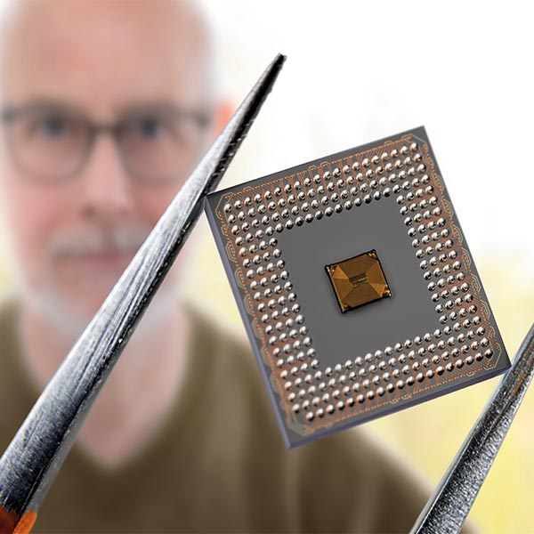
Embedded micro RFID tag in the rewiring of a chip for component identification and ensuring trustworthy supply chains | © Fraunhofer IZM I Volker Mai
Fraunhofer IZM is involved in several ZEUS research projects of the “Trustworthy Electronics” initiative of the German Federal Ministry of Education and Research.
Thank you very much for the interview!
¹ G. E. Moore: Cramming more components onto integrated circuits. In: Electronics. Band 38, Nr. 8, 1965, S. 114–117 (stanford.edu [PDF]).



Add comment