
In a world where technological innovation and environmental awareness must go hand in hand, Fraunhofer IZM-ASSID plays a leading role in developing sustainable cleaning methods for wafer-level packaging. As part of the Green ICT research project, research scientists are working to replace hazardous and environmentally harmful process chemicals with more environmentally friendly alternatives.
Dr. Maksym Myndyk, an expert in wafer cleaning at Fraunhofer IZM-ASSID, explains what is important in process analysis and how to substitute materials that are hazardous to humans or the environment in semiconductor manufacturing.
In the »Green ICT« research project, Fraunhofer IZM-ASSID is responsible for establishing alternative cleaning methods in wet chemistry for wafer level packaging (WLP) to reduce the reliance on environmentally harmful chemicals and establish or extend existing material cycles. To this end, the researchers analyzed various semiconductor manufacturing processes in order to replace selected chemicals with more sustainable options:
- Cleaning of Through Silicon Vias (TSV clean),
- Wet etching of metallic seed layers such as copper/titanium and silicon dioxide, and
- Removal of photoresists from wafers (photo resist stripping).
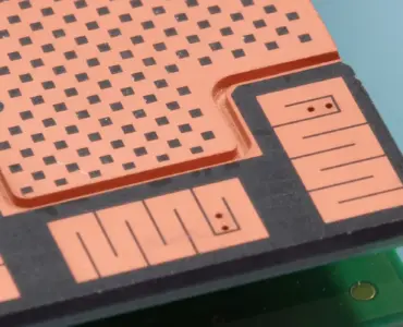
In electroplating, the seed layer is a thin layer that serves as a crystallization seed and adhesion base on a substrate during electrochemical deposition. It must be electrically conductive, but not necessarily closed.
The unprinted areas of the photoresist are removed, exposing the metal, which is then etched away. In wet etching, chemical solutions are used to convert solid material in the layer into liquid compounds.
Using material safety data sheets (MSDS), researchers at Fraunhofer IZM-ASSID have identified the chemicals that are hazardous to humans and the environment and should be replaced where possible.
Finding sustainable alternatives for fluoropolymer removal in Through Silicon Vias (TSVs)
Post-etch agents are commonly used in the industry to remove fluoropolymers from Through Silicon Vias (TSVs). These agents offer good cleaning performance, but contain hazardous chemical components. For example, EKC265 from DuPont contains the additives hydroxylamine, brenzcatechin, and hydroquinone, which are classified as carcinogenic under the REACH Regulation.
Benzcatechin is also mutagenic and very harmful to aquatic organisms. Wastewater must be treated separately and disposed of carefully. »Although this chemical is very well suited for semiconductor manufacturing, it is very difficult to handle and has negative effects on health and the environment,« says Dr. Maksym Myndyk.
Substituting a process chemical presents numerous challenges. »The chemical we have been using for the TSV cleaning process is ideal for this application and is well established in production,« explains Dr. Myndyk. Once a manufacturing process has been established, all production processes are essentially set in stone. Changing an existing process is very costly and time-consuming. In addition, the process must be reevaluated, as negative effects on product quality may occur later in the production process.
»The challenge in finding sustainable alternatives is that they should be both bioaccumulative and CMR-free (C = carcinogenic, M = mutagenic, and R = toxic for reproductive purposes), but also highly effective and cost-efficient,« says Dr. Myndyk. He is responsible for developing and establishing new processes in semiconductor manufacturing and investigating existing processes at Fraunhofer IZM-ASSID. His area of expertise includes wafer cleaning. He explains: »Cleaning the TSVs is crucial to avoid problems in subsequent processes.« One newly developed substitute is TechniClean BOS 390 from Technic France. According to the safety data sheet (SDS), it is non-toxic, non-flammable, and a nucleophilic mixture.

TSV process flow | @ Fraunhofer IZM-ASSID
The Green ICT project enabled researchers at Fraunhofer IZM-ASSID to test new process chemicals on the 200/300 mm wafer pilot line. As an expert in wafer cleaning, Dr. Maksym Myndyk works with EKC265 on a daily basis and is aware of its toxicity. »On the one hand, I am very interested in minimizing the health risk at my workplace. The chemicals currently in use are extremely dangerous for operators and the environment,« the research scientist warns. »On the other hand, the Green ICT research project gave us the opportunity to contact various chemical suppliers and discuss possibilities for cooperation.« Dr. Myndyk describes this as a win-win situation.
The researchers at Fraunhofer IZM-ASSID replaced EKC265 with the TechniClean BOS 390 and tested two cleaning processes. To ensure that the chemistry was compatible, the two TSV designs most commonly used at Fraunhofer IZM-ASSID were used: TSV 260 x 80 µm and TSV 100 x 10 µm. This involved collaboration with amcoss GmbH, which specializes in megasonic technology from ProSys.
A megasonic transducer couples acoustic energy into a liquid-filled gap formed by the substrate and the transducer surface. The shape and design of the resonator ensure uniform acoustic dosing across the entire surface of the rotating substrate without scanning motion.
»The road to a clean wafer was very long and not easy,« summarizes Dr. Myndyk. For each of the two cleaning methods, a large number of parameters must be defined and specified: prepare test wafers, run DoE, and analyze whether residues are still present. Different aspects of the TSVs, i.e., how deep they are etched and how wide their openings are, must be evaluated individually. How the cleaning process behaves with other designs would have to be tested and analyzed in each case. In order to replace chemicals, it is essential to examine the respective manufacturing processes, structures, and designs. Researchers have shown that alternatives and techniques do exist. »In our case, we evaluated the chemistry of the technology and assessed it for two designs. It worked. Personally, I think that’s a very good result.«
If photoresist remains on the surface of the silicon wafer after the Bosch process (reactive silicon ion deep etching), it must be removed. TechniClean BOS 390 can be used as a stripper and TSV cleaner in a single process step. Finally, both the photoresist on the wafer surface and the fluoropolymers from the TSV were completely removed. Adhesion analysis showed that this chemical is very well suited for this application. In a next step, a complete re-evaluation will be carried out together with the end customer.


260 x 80 µm TSV clean: The cleaned wafers were examined at several points using a scanning electron microscope (SEM). In particular, the walls and bottom of the TSV were examined for possible residues. | © Fraunhofer IZM-ASSID


The same method was used for TSV 10:1 structures. The proof that the TSV walls are free of fluoropolymers is provided by the visible etched »structures« (»scallops«). | © Fraunhofer IZM-ASSID
Update April 2026:
»We have supplemented our previous results with additional testing and verified the suitability of TechniClean BOS 390 for cleaning TSV structures with an aspect ratio of 10:1,« explains Dr. Myndyk in April 2026. After cleaning, the wafers underwent all subsequent process steps according to the POR, including dielectric deposition and the deposition of the titanium and copper seed layers.
The analysis was performed at three different locations across the entire wafer surface. The SEM images show no delamination or other defects, confirming the good compatibility of the cleaned surface with the subsequent dielectric. These results once again clearly confirm those previously obtained on TSV structures with an aspect ratio of 3.25:1.

SEM images of TSV structures following the CVD process and Ti/Cu PVD deposition. The good compatibility of the cleaned silicon surface is clearly visible on the TSV sidewalls. | © Fraunhofer IZM-ASSID


Detailed SEM analysis of the cleaned TSV structures to identify potential delamination and defects | © Fraunhofer IZM-ASSID

Close-up of the 10:1 TSV structures, consisting of silicon and silicon dioxide (dielectric), with layers of titanium, copper, and nickel built upon them | © Fraunhofer IZM-ASSID
In an online expert session at the end of 2023, Dr. Maksym Myndyk presented initial test results for a new sustainable material for cleaning TSVs made of fluoropolymer, which was produced using the DRIE process (Bosch plasma etching). More results are now available. PE-TEOS and seed layers such as metal, titanium, and copper were applied to the cleaned wafers. The wafers were processed in the same way as in pilot production, cross-sections were made of the wafers, and every micrometer of the TSV was analyzed from top to bottom to determine how good the adhesion is and whether there are any voids or delamination. This confirmed the good adhesion between the cleaned silicon and silicon dioxide.
»For us at Fraunhofer IZM-ASSID, this is the solution we have been looking for,« summarizes Dr. Myndyk. However, before pilot production at Fraunhofer IZM-ASSID can be converted and EKC265 replaced, discussions with the current cooperation partners and further practical tests are necessary. The purchase of a second cleaning system is planned for the new cleanroom at the Center for Advanced CMOS & Heterointegration Saxony. The chemical technology is to be used there. »Our goal is that the new machine never needs to use EKC265.«
Collaboration to develop environmentally friendly process chemicals for photoresist removal in microchip production
Photolithography is a key technology in the manufacture of integrated circuits (»microchips«). In this process, an image from a photomask is transferred to a photosensitive photoresist using an exposure process. Photoresists serve as temporary lithographic masks for structuring. The exposed areas are then dissolved. »The resist mask must be removed as quickly as possible and without leaving any residue. At the same time, neither the substrate nor the materials already deposited on it must be affected,« says Dr. Myndyk, describing the process.
Until now, Fraunhofer IZM-ASSID has been using an established solvent to remove photoresists from wafer surfaces. »This remover works very well, but it has the problem that it contains a dangerous additive that is just as toxic as hydrofluoric acid,« explains Dr. Myndyk. Even the smallest amount is lethal in direct contact with skin.
Fraunhofer IZM-ASSID has collaborated with a leading chemical company to analyze a TMAH-free (tetramethylammonium hydroxide) and environmentally friendly stripper that is still in development. The researchers prepared wafers with a copper seed, photoresist, and copper ECD pillars. The first generation of a stripper still in development was tested on a Semitool strip/etch annex to remove the photoresist. However, analysis of the wafer surface for possible residues showed that the copper removal rate was too high, which is counterproductive for the production of very fine structures. In consultation with the partner company, the second generation of the remover was further developed to optimize the copper removal rate. In a next step, test wafers with different resists, RDL structures, and copper pillars were stripped. Dr. Myndyk confirms that, with one exception, this has worked very well so far.
»Unlike large semiconductor fabs, we are able to test new chemicals on our production equipment,« says Dr. Myndyk, describing the research institute’s core areas of expertise. In consultation with the chemical suppliers, the respective chemical can be modified and re-evaluated as needed. »We help the manufacturers, and they help Fraunhofer IZM-ASSID. It’s a win-win situation for both sides and for the environment!« All processes tested at Fraunhofer IZM-ASSID run on industrial equipment. This ensures that customers can quickly transfer these processes to their own facilities later on.
This post was updated on April 16, 2026, and now includes detailed REM images and information on the current state of research.


Add comment