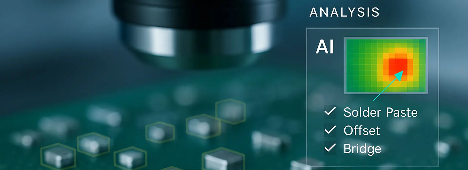
How well the assembly of Surface Mount Device (SMD) is done determines the performance, reliability, and longevity of the resulting electronic systems. This is why quality assurance in electronics manufacturing includes key processes like solder paste inspection (SPI) or automated optical inspection (AOI). Although both processes deliver precise results, they have largely been run separate from each another. As a result, errors – for example, in solder paste printing – are often detected too late and are not interpreted across processes.
In his master’s research, Karim Shousha from the »Photonic and Plasmonic Systems« working group at Fraunhofer IZM is investigating how an AI-supported analysis of SPI and AOI data could be used to implement a coherent inspection workflow that not only detects defects in PCB assembly, but also explains them in a manner that can be understood.
To this end, he tested various AI models – from conventional image recognition to large language models (LLMs) and multimodal solutions – for their suitability for cross-process error analysis. His investigations led him to several clear statements about practical feasibility and the appropriate model selection.
In his interview with RealIZM, he provides some insights into his findings and highlights the potential that AI-supported inspection methods could offer for SMD assembly.
RAG-supported pipeline for SPI and AOI data
Manufacturing defects in the soldering process – such as bridging, voids, or displaced components – are among the most common causes of failures in electronics manufacturing. Focusing on solder paste inspection (SPI) and automated optical inspection (AOI), Karim Shousha has designed an AI-supported pipeline architecture that combines both inspection methods in a single integrated workflow. This can improve the quality and reliability of assembled printed circuit boards and extend their service lives.
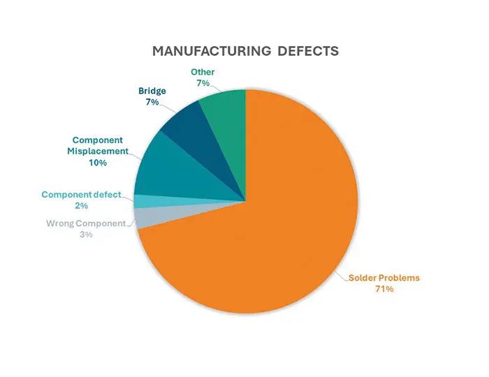
Approximately 70 percent of manufacturing defects occur during soldering | © Fraunhofer IZM | Biemans: 5D solder paste inspection–merits beyond 3D technology. In: Global SMT & Packaging (2011), S. 8.
The key finding of his research is that the most promising approach for inspection in industrial PCB assembly is neither conventional image processing nor a large cloud-based AI system, but rather a compact, locally operable AI model that is specifically enhanced with domain-specific knowledge using retrieval-augmented generation (RAG).
At the core of the pipeline is the Vision Language Model (VLM) Qwen3-VL-8B, which was released in the fall of 2025. As a multimodal AI model, it can process and interpret high-resolution image data together with textual information. It recognizes electronic components, analyzes their position on the circuit board, and precisely identifies defects.
By adding RAG, the system can also access IPC standards, Gerber data, and process-specific metadata before analysis. This allows industrial quality requirements to be reliably evaluated – an advantage that would not be achievable with purely data-driven models alone.
Deep learning as a basis: Strengths and weaknesses
Today’s AI landscape is characterized by a multitude of models that essentially differ in two dimensions: their capabilities (e.g., detection, understanding, and reasoning) and their size – the scope of the training data and parameters used. »To determine a suitable approach for the automated detection and classification of PCB components, that made it important to systematically examine different AI model classes,« Shousha says about his approach.
The focus was on deep learning models: They form a subcategory of machine learning and are based on multi-layered artificial neural networks that learn patterns directly from large data sets, instead of following hard-coded rules. Deep learning forms the basis of many modern AI processes, such as image and speech recognition or word processing.
The central challenge lies in the data sets required for model training. Karim Shousha emphasizes: »The significance of deep learning systems is directly linked to the training and test data sets used. Since these are often proprietary in specialized domains like electronics manufacturing, they are not transparent and we cannot assume the data coverage to be complete or that test results can be validated in an unrestricted and properly traceable way.«
Model comparison: YOLO, zero-shot, and large models
The multi-stage testing process included various deep learning models – from more specialized, task-specific approaches to more general and powerful architectures. The first step was to use YOLO-based models (»You Only Look Once«), which enable the efficient localization of components through visual object recognition. However, their weakness lies in their dependence on extensive, annotated data sets.

Comparison of four tested AI models | © Fraunhofer IZM

Recall and precision of different tested AI models | © Fraunhofer IZM
In the next step, Shousha investigated zero-shot vision-language models. These link visual content with textual descriptions and recognize objects without explicit task-specific training. Although they are based on vision-language architectures that process image and text information together, they reach their limits when the data in the pre-training does not sufficiently cover the target domain, such as electronics or PCBs. Finally, Shousha tested large-scale models – large language models (LLMs) and visual language models (VLMs).
Large versus small AI models: Performance, costs, and data protection
The size of an AI model is determined by the number of its parameters – the trainable weights used to learn patterns in data. Small AI models have around 1 to 10 billion parameters. Large AI models, on the other hand, work with up to 500 billion parameters or more. LLMs and VLMs of this size offer powerful recognition and reasoning. The downside is that they require more computing power, consume more resources and bring more deployment and inference costs.
In addition, aspects of data security and reliability play an important role: large AI models are provided via clouds. This makes it difficult to handle sensitive production data and poses additional security challenges. So-called hallucinations also pose a problem: AI models can generate false or unverifiable statements, often with a high degree of confidence, for example due to insufficient context, ambiguous prompts, or a lack of reliable grounding.
Against this backdrop, locally operated, closed AI systems seem to be the most suitable for contract manufacturers, as Karim Shousha explains: »Protecting sensitive manufacturing data is a high priority. Therefore, many companies prefer closed networks.« Such solutions are also economically advantageous, as operating large AI models trained with billions of parameters involves considerable costs and is difficult to scale efficiently in practice.
However, using smaller AI models also has its limitations: they may be easier to implement and cheaper to operate, but compared to large AI models, they often deliver lower performance.
Optimized inspection workflow through RAG
The necessary compromise between data sovereignty and system performance, which becomes so apparent when using smaller AI models with limited capacity and a lack of domain knowledge, can be circumvented by implementing a RAG. Tests of the existing inspection workflow showed that this approach strikes the middle ground between high model performance and practicality. This means that even compact VLMs like Qwen3-VL-8B can be expanded to achieve almost the same performance as significantly larger AI models in PCB inspection. This approach is particularly promising for SMD assembly and can be easily integrated into existing SPI/AOI lines.

Simplified representation: Workflow from image processing to AI model processing | © FRaunhofer IZM
»The key advantage of this pipeline,« Karim Shousha explains, »is that it not only detects defects, but also explains their causes. AI-supported data analysis shows at which stage of the process the defects occur and opens up the possibility of making just-in-time corrections in the manufacturing process.« In the long term, electronics manufacturing service providers could benefit from real-time monitoring in a live production environment, where errors can be detected and corrected immediately after they occur.
»Cause identification, not just fault detection: AI-supported data evaluation […] opens up the possibility of making just-in-time corrections in the manufacturing process.«
Karim Shousha, Student Assistant, Fraunhofer IZM
Test results: Fault detection in the laboratory
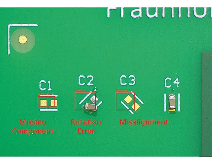
The workflow was tested on the Start-a-Factory prototype line at Fraunhofer IZM. Ten test circuit boards (60 mm × 60 mm) with placement and printing errors deliberately incorporated were used to cover a representative range of fault categories. The RAG-supported VLM model detected the defects and provided a structured output of the error analysis, from visual details to the position and type of error.

Test PCB with built-in printing errors – missing component and misalignment. | © Fraunhofer IZM
Test PCB: Error detection – Claude Sonnet 4.5 | © Fraunhofer IZM
Outlook: Potential for production and automation
AI-supported inspections can go beyond the purely rule-based error detection of conventional inspection systems. They add flexibility, interpretability, and adaptability to new PCB layouts. The model’s structured JSON output can be fed into machine communication. This allows manufacturing processes like PCB assembly or solder paste printing to automatically respond to and correct identified defects. AI-supported workflows can, in principle, be adapted for any production line.
Use in photonic housing manufacturing
The research work was carried out in the »Photonic and Plasmonic Systems« group, because it addresses key challenges that arise in both microelectronics and photonic manufacturing. Similar to electronic assemblies, photonic and plasmonic systems require high-precision manufacturing and assembly processes in which even the smallest deviations in component placement or classification can significantly impair their functionality. »The AI workflow for printed circuit boards can also be implemented in photonic housing manufacturing,« Karim Shousha explains.


Add comment