How can the production quality of geographically dispersed electronics production lines be reliably monitored in real time? The BMFTR-funded research project AdaPEdge addressed this question. The goal was to digitally capture environmental, production, and machine data at various locations and analyze it using artificial intelligence (AI). The focus was not on individual electronic components, but on the quality level of entire production lines.
Steve Voges, process development engineer, and Karl-Friedrich Becker, group leader of »Assembly & Encapsulation« at Fraunhofer IZM, spoke with RealIZM about the development and added value of the new evaluation metric »Condition Level Monitoring«.
From Yield to »Condition Level«
»The quality of manufacturing environments is often assessed retrospectively using metrics such as yield or process control charts for individual process steps,« summarizes Karl-Friedrich Becker. »The AdaPEdge project takes a different approach: It relies on a new evaluation metric – so-called Condition Level Monitoring.«
The »Condition Level« describes the aggregated quality status of an electronics production line. It is derived from the comparison of a wide variety of data sources – such as environmental, machine, process, and quality data. The goal is to detect deviations from the optimal state early on and to initiate automated countermeasures.
»The best state of a production line is the most efficient one. It is associated with low scrap rates and high yield and serves as a benchmark for quality control. Efficiency is no accident – it is measurable.«
Karl-Friedrich Becker, Group Manager »Assembly & Encapsulation«, Fraunhofer IZM
This makes the Condition Level a key management tool – both for internal operations and for communication with customers.

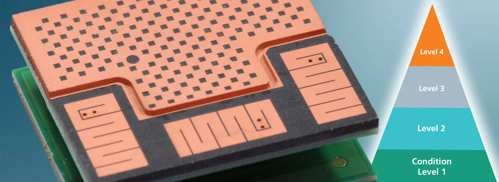
The »Condition Level« is an independent, standardized evaluation factor for the resilience and robustness of manufacturing, e.g., to reduce inspection intervals or increase them in the event of a failure | © Fraunhofer IZM
Learning Across Locations – Without Losing Data Sovereignty
A central element of the AdaPEdge project was federated learning. The basic idea: Different manufacturing sites learn from one another without having to share their raw data in full. Each site analyzes its own local data and shares only aggregated information. This information is then consolidated into a single model and analyzed using AI.
This approach addresses one of the biggest challenges of distributed manufacturing: data sovereignty. Companies retain control over which data they share. At the same time, they benefit from the knowledge of other sites.
»Federated learning makes it possible to combine and comparatively evaluate reduced datasets without allowing detailed conclusions to be drawn about individual sites,« says Steve Voges. »In this way, overarching quality patterns can be identified without disclosing sensitive production data.«
Video © Strategische Partnerschaft e.V.
Sensor Technology, Edge Computing, and Data Fusion
Comprehensive and continuous data collection is essential for reliably determining the condition level. For this purpose, the AdaPEdge project established extensive sensor infrastructures on both the Fraunhofer IZM prototype production line and the industrial production lines of Siemens AG (project coordinator) and Micro Systems Engineering GmbH (project partner).
Mesh-capable sensor nodes developed specifically for the project were deployed at various stations along the distributed production lines. These multisensor modules measure parameters such as temperature, humidity, and acceleration. The data is then transmitted wirelessly to an edge computing module.
There, the data is preprocessed and time-stamped. All information is time-stamped and stored in a database that serves as a data lake. This makes it possible to determine which environmental conditions prevailed at which machine at a specific point in time later on. This transparency is crucial for identifying the causes of quality deviations.

Schematic representation of the sensor infrastructure of the AdaPEdge network at Fraunhofer IZM | © Fraunhofer IZM I Steve Voges
Cost-effective sensor technology for retrofitting existing production lines
»One of the project’s objectives was to develop a cost-effective, retrofittable sensor system,« explains Becker. »The sensor nodes are therefore deliberately designed to be compact and versatile.«
The S³EM sensor mesh technology, which uses integrated edge computing modules, enables decentralized communication and the forwarding of measurement data within the sensor network. The modular design of the network supports scalable expansion through additional sensor nodes.
A standardized MQTT protocol ensures easy integration into any production environment. The system is particularly suitable for retrofitting production lines that have been largely undigitized to date. It enables continuous process monitoring as well as data-driven quality assurance and improvement.
Sensorik Bayern GmbH was responsible for the system design of the sensor nodes. Fraunhofer IZM and TU Berlin developed an industrial-grade multisensor module as well as the associated 3D antennas: a 2.4 GHz RF design featuring 3 switchable metallized antennas on the mold and 5 shielded sides plus 1 side with a shielding trench. The antenna design is optimized for high efficiency in harsh industrial environments and combines a novel antenna technology with shielding approaches integrated into the packaging.


Package with shielding, RF antenna, and sensor integration: first-generation S³EM (left) and third-generation S³EM | © Fraunhofer IZM
To optimize electromagnetic compatibility (EMC), the shielding mechanisms were analyzed at the project partner TU Berlin. For this purpose, an automated test bench was developed and evaluated to determine the shielding effectiveness (SE factor) and to analyze potential interference within the Secure Smart Sub-Edge Modules (S³EM). »The Secure Smart Sub-Edge Modules are shielded against external EMC influences. Full encapsulation additionally protects the hardware from potential tampering,« explains Steve Voges. Furthermore, a crypto chip can be integrated to enable encrypted communication and authentication. This security architecture was already successfully implemented in the predecessor project »SieVei 4.0«.

Schematic representation of the SE factor measurement setup: Broadband measurement of the SE over a wider frequency range in a single run – 10 MHz to 1 GHz and beyond (left) | © TU Berlin I Lukas Becker (right) © Fraunhofer IZM I Steve Voges
Advances in Packaging and EMC Shielding
In addition to the data layer, the hardware also played a central role. Fraunhofer IZM and TU Berlin jointly developed a packaging concept for the sensor nodes with the goal of shielding the modules as effectively as possible against electromagnetic interference.
During the course of the project, it became apparent that using the method previously employed at Fraunhofer IZM the metallization did not adhere sufficiently to the mold compound. »To improve the shielding of the package, we switched the process from sputter metallization to direct metallization,« explains Becker.
The evaluation of the layer adhesion of metallization on mold compounds was also scientifically supported as part of a master’s thesis. »As a result, we now have significantly better metallization and a very good evaluation method. This is another great success for us in this project,« Becker summarizes.
Real-Time Response to Anomalies
The true value of Condition Level Monitoring becomes apparent during ongoing operations. If the condition level drops below defined thresholds, the system responds automatically. It triggers alarms, visualizes the status of the production line, and provides operators with a solid basis for decision-making.
»Inspection intervals can be dynamically adjusted using ›Condition Level Monitoring‹. Reduce them during stable periods and increase them specifically when anomalies are detected. This makes production more transparent, resilient, and robust.«
Steve Voges, Process Development Engineer, Fraunhofer IZM
The Role of AI in the Project
The University of Bielefeld was responsible for the AI-based analysis of the collected manufacturing data to assess the condition level. There, the AI was selected and adapted to be suitable for use on edge computing modules directly on the production floor – without the need for high-performance computing. To implement a cost-effective, retrofittable sensor system, a resource-efficient AI was required that pre-compresses and pre-evaluates the data.
In addition, AI was used to tap into new data sources along the production lines. »We investigated which parameters in the molding process had not been recorded until now,« Voges explains. Using a camera and AI-supported analysis, the geometries of the dispensed mold compound were captured as a 3D image. »These additional sources of information enable us to evaluate the process even more precisely.«
Follow-up Project and Outlook
The approaches developed in the AdaPEdge project are being incorporated into further research initiatives. In the CHOPS project, for example, design and packaging flows for electro-photonic systems are digitally described and integrated into open-source design software such as KiCad as an Assembly Design Kit (ADK). The basis for this is the System Technology Co-Optimization (STCO) approach, in which design and technology are considered together from the very beginning. Among other things, the plan is to provide an open PDK for PICs and to map advanced packaging (3D AVT and Fan-out Wafer Level Packaging (FOWLP)) in the OS design tool. Developers of photonic assembly and interconnection technology could thus verify as early as the design phase whether a product is manufacturable. An AI-supported design rule check helps to avoid errors early on and bridge the gap between chip, package, and system.
Event Notice
As part of the »FANOPa« project, funded by the Berlin Senate, Fraunhofer IZM has developed a fan-out wafer-level packaging platform for RF applications. Fundamental investigations into the FOWLP process were conducted to determine chip displacement during the encapsulation process based on historical process and material data. Thanks to the process models developed, exploratory trials are now rarely, if ever, necessary.
»With the AdaPEdge project, we were able to demonstrate how AI, sensor technology, and federated learning can be meaningfully combined to holistically assess quality in distributed manufacturing,« Voges summarizes. »Condition level monitoring not only enables transparency but also rapid, automated responses to deviations. In this way, the project makes an important contribution to resilient, data-driven electronics manufacturing in the spirit of Industry 4.0.«
AdaPEdge: Edge computing modules for resilient electronics manufacturing with adaptive process optimization
Funding Code | FKZ 16ME0547K |
Funding Agency | Federal Ministry of Research, Technology and Space (formerly Federal Ministry of Education and Research) |
Funding Amount | €4.6 million BMFTR funding: €2.98 million (65%) plus €0.15 million in so-called project stipends for participating universities |
Duration | July 2022 – December 2025 |
Project Lead | Siemens AG |
Project partners | Universität Bielefeld Sensorik-Bayern GmbH Creonic GmbH Fraunhofer IZM Technische Universität Berlin Micro Systems Engineering GmbH Miele (associate partner) |
Project website |


Add comment