Hermann Oppermann from Fraunhofer IZM, Norwin von Malm and Stefan Grötsch from ams OSRAM jointly received the Deutscher Zukunftspreis 2024 (German Future Prize) for the development of the high-resolution LED matrix technology »Digital Light«. This innovative lighting technology enables precise, energy-efficient, and dynamic control of vehicle headlights.
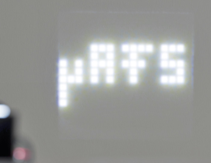
In an interview with RealIZM, Hermann Oppermann shares insights into the technical challenges involved in developing the intelligent lighting solution, milestones of the »µAFS« research project, and potential applications of digital light.
First of all, congratulations on winning the Deutscher Zukunftspreis 2024! What feedback and inspiration have you received since the award ceremony?
Hermann Oppermann: Our team was delighted to receive this award. The Deutscher Zukunftspreis is an important recognition of the work of all researchers in the field of digital light technology – it is a strong motivation for us to continue making progress. For our research institute, it is an excellent example of how we transform ideas into products and make our applied research visible to the general public.
The Deutscher Zukunftspreis is one of the most prestigious awards for applied science and technology in Germany. It is awarded annually by the German Federal President and comes with a prize of €250,000. The award honors technical, engineering, and scientific achievements that have already resulted in application-ready products.
This marks the tenth time that the Fraunhofer-Gesellschaft has been awarded the Deutscher Zukunftspreis. In 2024, Fraunhofer IZM was honored for the first time.
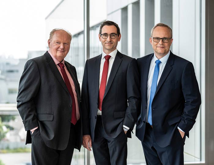
Left: From left to right: Hermann Oppermann (Fraunhofer IZM), Norwin von Malm (ams OSRAM), Stefan Grötsch (ams OSRAM) | © Deutscher Zukunftspreis | Ansgar Pudenz
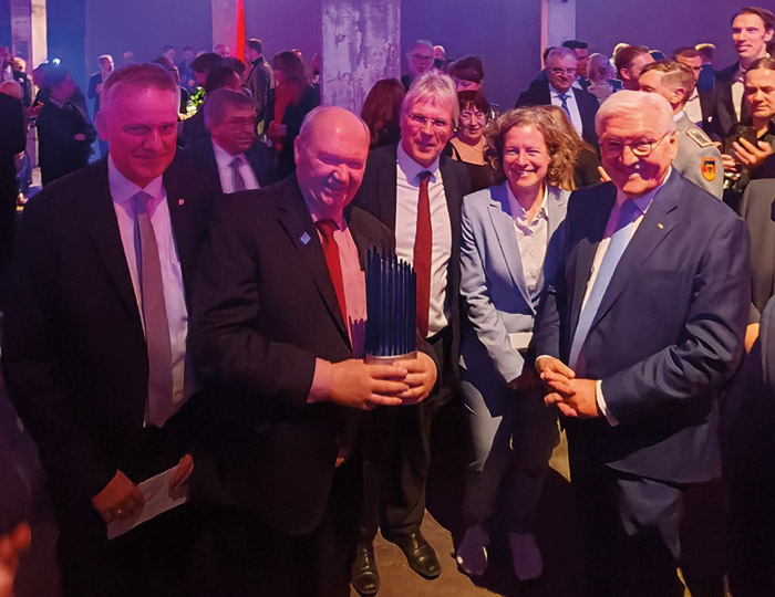
Right: Prof. Martin Schneider-Ramelow, Hermann Oppermann, Prof. Holger Hanselka, Prof. Ulrike Ganesh, Federal President Frank-Walter Steinmeier | © Fraunhofer IZM
What was the µAFS research project about and what is the idea behind it?
Hermann Oppermann: Until now, car headlights could only switch between low beam and high beam. To increase driving safety at night, we needed headlights that could illuminate the road more flexibly, without dazzling oncoming traffic. Early concepts allowed segmented dimming and brightening.
With LEDs, multiple segments became possible, but the light distribution was still too coarse. The goal was to achieve highly precise control of light zones in a very compact space to illuminate the road optimally in any given situation.
Research project »µAFS«
The abbreviation µAFS stands for integrated μ-structured light-emitting diodes as intelligent light sources for innovative adaptive headlight systems.
Funding body: Federal Ministry of Research, Technology and Space (formerly BMBF)
Duration: 02/2013 – 07/2016
Project partners:
Daimler AG, Hella KGaA Hueck & Co., Infineon Technologies AG, OSRAM GmbH, OSRAM Opto Semiconductors GmbH, Fraunhofer IAF, Fraunhofer IZM
Press release on the project
What technical challenges did Fraunhofer IZM face?
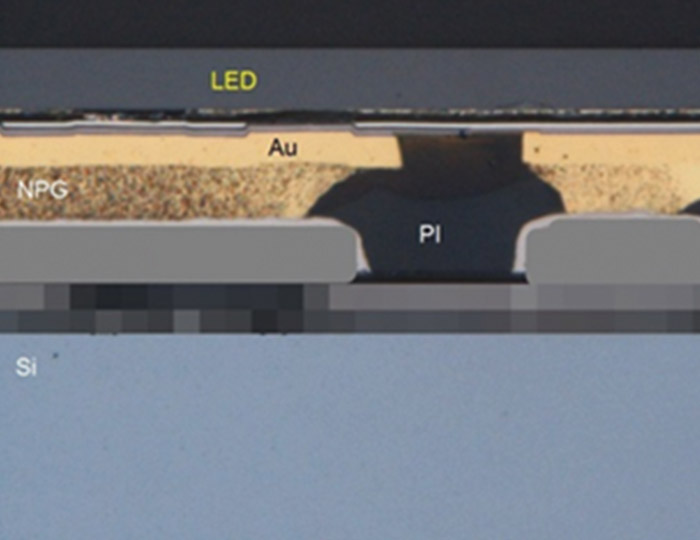
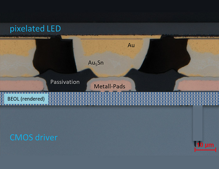
Hermann Oppermann: OSRAM had already developed a pixelated LED light source and a CMOS model. However, controlling the LED matrix required a large number of data lines. OSRAM therefore sought a research partner to support implementation. The main challenge was to reliably supply high currents to the LEDs and dissipate the resulting heat loss of up to 40 watts.
Since the light passes through a converter layer on top of the LED, cooling was only possible via the already heat-stressed CMOS chip. That meant we needed a robust interconnection that could conduct high currents, avoid electromigration, and effectively dissipate heat through the CMOS chip via the circuit board.
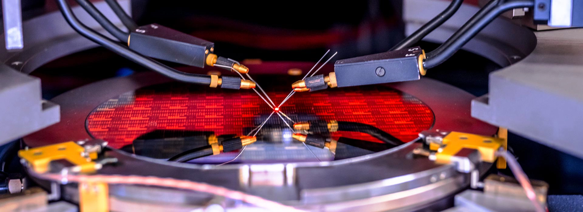
At the start of the project, the specifications were clear: the LED chip was to have a total of 1,024 pixels, each pixel measuring 125 µm with defined current and power dissipation. What was unclear was which materials and which bonding processes would work: Could soldering be used, or was underfill necessary? We were tasked with evaluating the options and were offered the prospect of a BMBF-funded project.
What technological solutions were examined and which process prevailed?
Hermann Oppermann: At Fraunhofer IZM, we considered several baseline technologies. In the end, two approaches made it into the final selection: a gold-tin alloy and a nanoporous gold structure. The gold-tin alloy is a proven soldering process, but at that time had not been applied in fine-pitch areas with such high contact density. We were asked to achieve spacing of 15 µm on the LED chip. We decided on this approach because it is stable at high temperatures, reliably conducts high currents, ensures efficient heat dissipation, and is easy to process.
As a second approach, we chose a nanoporous gold structure. This sponge-like material can be compressed and adapted precisely to the component’s topography. At the time, it had hardly been used, but we were able to further develop it and demonstrate feasibility.
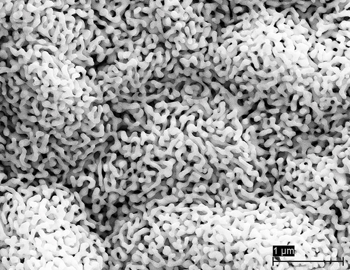
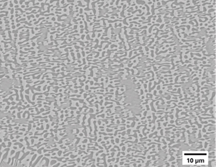
Left: Nanoporous gold forms a sponge-like structure with approximately 70% porosity
Right: Microstructure of eutectic AuSn solder | © Fraunhofer IZM
To control each light point independently, gold nanosponge (left) or AuSn solder (right) establishes contact between the individual pixels and the driver chip. | © Joint final report µAFS
Ultimately, the gold-tin alloy was chosen, as it was the more predictable and established process.
How was the first µAFS demonstrator constructed, and what technical challenges did your team face?
Hermann Oppermann: In our initial approach, we connected four 2 x 2 mm LED chips, each with 256 pixels, to the driver electronics chip, creating a demonstrator with a total of 1,024 pixels. In practical tests, however, visible transitions between adjacent arrays became apparent, forming a cross pattern on the road. This was not well received by motorists.
It should not be forgotten that chip technology was also being further developed in parallel with the development of the LED headlight. The dimensions of the LED chip were later adjusted to 4 x 4 mm in order to optimally illuminate the desired light cone and model the light pattern more finely.
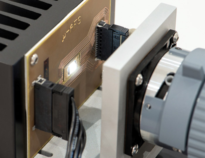
The demonstrator developed by the consortium partners was the first step toward even smarter LED headlights in the future. | © OSRAM
The first µAFS demonstrator shows that 256 pixels can be individually controlled using just one LED chip. © OSRAM
Were there additional challenges?
Hermann Oppermann: Manufacturing novel LED structures with high yield is inherently difficult. In the first year, since CMOS chips were not yet developed, we mounted the first LED pixel arrays on a hard-wired silicon circuit. When they lit up permanently, the excitement in the team was huge.
However, we quickly realized that we had not thought far enough ahead in the project. Follow-up processes at wafer level were necessary for series production. In spring 2015, we applied for additional funding from the BMBF to adapt the technology to wafer-level assembly.
The pixelated LED chip used later in the project consisted of a gallium nitride base grown on sapphire. When such an LED chip is mounted and bonded to a Si-based CMOS chip, there is a difference in the coefficient of expansion. At the time, it was unclear whether it would be possible to reliably bond the LED chip of this size to silicon, because the combination and the mounting process were still very new at that time.
Was it surprising to realize you had underestimated the scope?
Hermann Oppermann: In early development phases, you always try out different approaches and explore feasibility. It was only when we committed to developing a product for series production that the full extent of the required steps became clear.
How did product development affect your everyday work?
Hermann Oppermann: It became very concrete. We suddenly had a lot of material to process. For my working group, it was a dream come true to be so closely involved in the development of a specific product. We were able to standardize processes and implement them in our clean room with a very high yield. This greatly increased the confidence of the project partners and demonstrated the importance of interdisciplinary collaboration in driving innovation. Product-oriented thinking is fundamental to research projects, but it is not always feasible. Ultimately, it depends on the market situation and the competitive environment. What we achieved with the »µAFS« demonstrator was unique and had never been done before. Looking back, our step-by-step approach was exactly right: we achieved early successes at the chip level before scaling the technology to the wafer level.
What advice would you give to research teams?
Hermann Oppermann: My recommendations to project partners are: Identify the truly critical development steps early on. Test and validate them thoroughly. Only once the key processes are mastered should scaling begin. This minimizes risks and quickly provides certainty as to whether the chosen path will lead to the desired project goal, or whether an alternative solution should be pursued.
What particularly stayed with you from the µAFS project?
Hermann Oppermann: The moment I remember most vividly was seeing the first blue pixel array without a converter. It wasn’t just the light itself that was impressive, but above all the light output – we’re talking about almost 4 lumens per pixel, meaning up to 4,000 lumens from a 4 x 4 mm chip. At the time, three such chips were used per spotlight, enough to illuminate an entire lane.
How did the first practical test go and what insights were gained?
Hermann Oppermann: Our LED arrays, mounted on CMOS wafers, were further processed at OSRAM, mounted on a circuit board, and equipped with a cooler. Hella integrated the system into a headlight with a lens, which was then installed in a vehicle. Daimler took care of the control and switching. In early 2016, during a test drive at Daimler’s site, we saw the headlight pattern on the road for the first time.
It was immediately clear this was something special. As mentioned, the cross structure of adjacent arrays was still visible, but the live experience was invaluable and ultimately led to the shift to 4 × 4 mm LED chips.
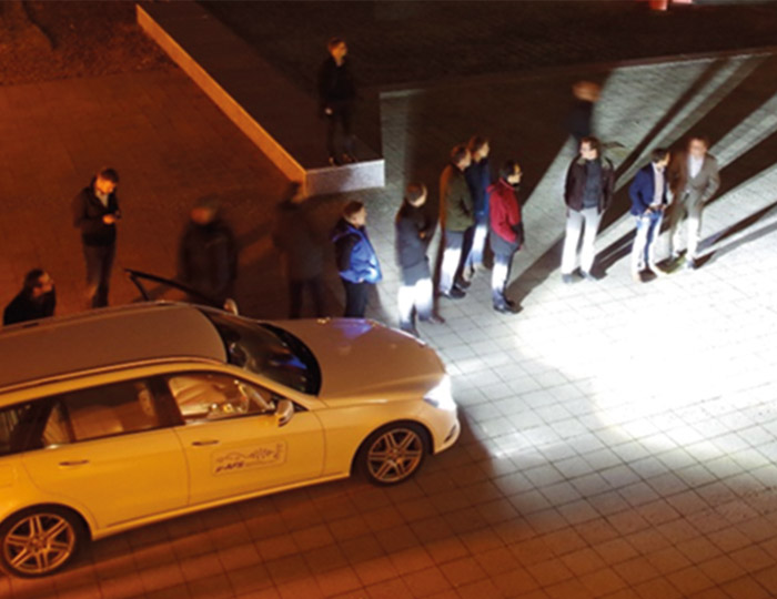
Ready-to-run test vehicle at the project meeting on February 22, 2016, Ulm. | © Final report µAFS
Why did the µAFS project start with 1,024 LED pixels, even though the series product uses 25,600 LED pixels?
Hermann Oppermann: At the time, we provided the basic technology for the µAFS project and, once the project was complete, transferred all the processes and technologies developed to OSRAM as part of a transfer project. This allowed our partner to integrate them into production. For us, this was an important milestone.
The subsequent scaling from 1,024 pixels to a series-ready product with over 25,600 pixels was achieved by ams OSRAM in close coordination with automotive industry requirements.
What added value does »digital light« LED matrix technology offer in road traffic?
Hermann Oppermann: LED matrix headlights can adapt automatically to traffic conditions. They selectively dim areas to prevent dazzling oncoming or preceding vehicles. while illuminating traffic signs in a targeted manner to make important information more visible.
Similar to a video projector, warning symbols can also be projected onto the road, for example in the form of a snowflake. Lane changes can be indicated by arrows, and in narrow construction zones, the projected vehicle width helps drivers assess available space. These features increase both driving safety and comfort, offering drivers reliable adaptive light control at all times.
© OSRAM
What other applications are known or conceivable for precise, adaptive lighting control?
Hermann Oppermann: A promising field is augmented reality (AR), where images are projected directly into the user’s field of vision. To achieve this, even smaller LED pixels and even smaller distances between the pixels are required. While white light patterns are sufficient for vehicle headlights, AR projections require the three primary colors red, green, and blue. Therefore, research is focusing on compact RGB LED modules.
Even though the µAFS project has been completed, the research field of digital light – from AR applications to optical data communication between computer chips in data centers for AI applications – continues to offer great development potential.
At Fraunhofer, PrePAre projects such as »µLED Assembly« are developing the underlying technologies for microdisplays and augmented reality. The BMFTR-funded project »Silhouette« is making silicon-based photonic technologies accessible for applications in the field of security solutions for open processor systems.
Thank you very much for the interview and continued success!
Podcast: Digital light – LED technology nominated for the Deutscher Zukunftspreis
(Podcast language: German)
Interview: Dr. Hermann Oppermann, Fraunhofer IZM, Dr. Norwin von Malm, and Stefan Grötsch, ams OSRAM | November 19, 2024


Add comment