Progressive digitalization driven by advanced assembly and packaging
Digitalization is happening right now in almost all areas of our world. With increasing numbers of end products getting connected, more and more custom systems are required to run them – with often such specific, custom properties that only small numbers are produced to meet actual demand. This poses a new challenge for commerce, but even more for the development processes and the system integration technologies used.
System integration technologies themselves need to evolve in terms of their technology and processes in order to increase productivity and keep costs low. With integration technologies at wafer-level or panel-level, solutions are rapidly developing that permit unparalleled miniaturization at all production volumes common in the market.
A major trend in digitalization is the interconnection of all devices, including a multitude of everyday objects, which is why we are talking about the Internet of Things (IoT). We can already see radical changes in the form of smartphones, electronic ID cards, smart wristbands, or networked bicycles and cars. Medical technology is also increasingly relying on tiny electronic components to offer a level of help and comfort for people that seemed unimaginable just a few years ago, but seems indispensable now.
The people making, selling, and using these applications tend to take one thing for granted: The constant availability of miniaturized, multifunctional, and autonomous electronic systems that can record, process, and transmit data or influence the systems and communication networks controlled by them.
What do we expect from smart electronic systems?
For them to power the process of digitization and the Internet of Things, electronics need to become increasingly powerful, energy-efficient, and multifunctional, while still staying as cheap and economical as they can be. This requires a large number of disruptive innovations at all levels of digitization, made possible with electronic components, intelligent firmware, and new interface architectures geared to specific application needs.
The number of networked components in the Internet of Things is growing extremely fast. From 2025 onwards, networked sensor nodes are expected to multiply at an exponential rate. The problem here is that energy consumption will continue to rise with the number of nodes. According to a study by the International Energy Agency, the power hunger of all networked devices worldwide in 2013 matched the total demand for electrical energy in Germany. Within the next few years, this is set to almost double to 1140 Terawatts per year as a result of digitalization. The Internet of Things is playing a particularly significant role in this growth.
For this reason, it is important for smart electronic systems to become much more energy efficient and for the applications they control to be more economical with the energy they use. Energy optimization must take place at every functional level as well as in the system as a whole. All options for energy efficiency must be considered in any system’s development from the very first conceptual ideas. This applies to the entire signal chain from sensor operation, signal conversion, energy management, and the network technologies used in the finished system.
Intelligent circuit design and optimized algorithms for data processing and the use of suitable networks with the lowest latencies and the highest quality of service ensure that functions can be provided with the lowest possible energy consumption needed to operate the application. Energy harvesting systems are also an option for generating and storing power on site to maximize uptime and, where necessary, eliminate the need for external batteries, making the system fully energy self-sufficient for its effective lifetime. Broadband multi-energy harvesting from the environment, energy storage for long operating times without needing battery replacements, and operating lives maximized by minimizing control loops to shorten reaction times and energy-consuming data transfers play a decisive role here.
Increasing miniaturization now makes it possible to build extremely small batteries and connect even the smallest objects with each other. With the current trend towards larger substrate formats, production costs can be kept low despite different production volumes. wafer level (e.g. Fan-out-WLP) and panel level packaging (e.g. Fan-out-PLP) are some of the latest assembly and packaging trends in the system-in-package world, responding to the increasing call for extreme system miniaturization.
WLP and PLP-based system integration
Miniaturization and much higher performance were essentially made possible by specific types of wafer level packaging (WLP). These packages currently account for around 50 percent of active components in modern smartphones, set to rise further and rise rapidly. However, such WLPs often only have a dimension close to the chip size itself (Chip Size Package), making it extremely difficult to achieve greater complexity in 2D. Further development will therefore focus, among other things, on three-dimensionality (e.g. by through-silicon vias). In addition, the constant miniaturization of IC structures is now making it increasingly difficult to distribute solder balls over the entire surface of a pitch, which enables subsequent assembly on standard printed circuit boards.
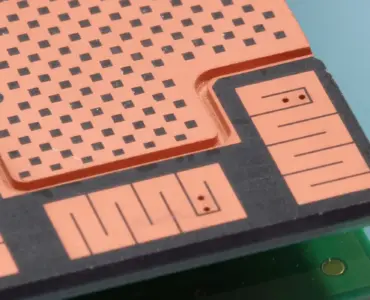
Another promising development is Fan-out WLP, which allows connections through the redistribution layer beyond the chip area. As a possible process sequence, the wafers are singulated and the ICs are glued onto a temporary foil with the active surface facing downwards. The ICs are overmolded with the molding compound from the back. Once the foil has been removed, the redistribution layer can now be built up. Fan-out WLP is the ideal connection between a package without substrate and the possibility to distribute the chip area for the SMD grid using highly filled epoxy resin. In contrast to the previous WLP, where rewiring is only possible within the IC (Fan-in), it is now possible to adapt the connection layout, so that further system integration steps can be taken at the package level. Further ICs, passives, and other components can be integrated into the package, so cost-effective system-in-packages (SiP) can be realized directly in the package itself. This avoids cost-intensive interposers for layout adaptation. Until now, processing has largely been carried out on 300 mm wafer formats, which can be extended to a maximum of 330 mm.
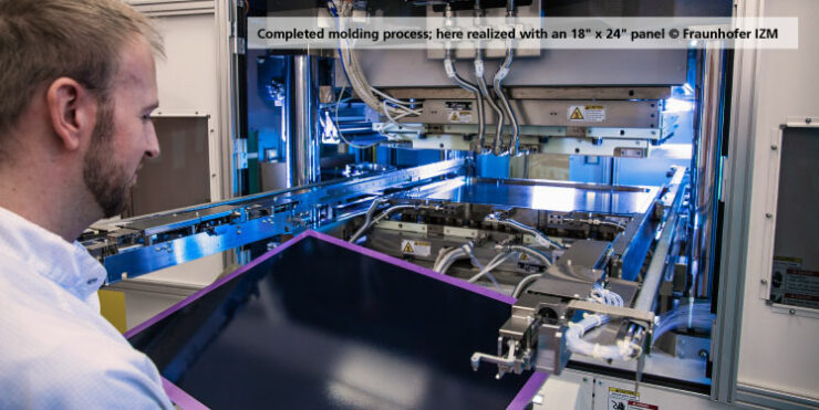
Another approach is the use of large-area panels (substrates: printed circuit boards or moldings), as are already used in LCD and solar applications. When Fan-out WLP processes are converted to such large panels (Fan-out Panel Level Pacakging) with different formats (e.g.18 x 24 inches), manufacturing costs can be further reduced. However, while the processes for wafer level packages are largely standardized, panel technologies are still undergoing process and system development to ready them for industrial mass production.
The disadvantage is that it is usually not possible to simply adopt the familiar wafer level materials, technologies, and standards. This is another reason for why a worldwide consortium (Panel Level Packaging Consortium) was founded on the initiative of Fraunhofer IZM to investigate questions of cost modelling and technology optimization in the areas of assembly, redistribution, and molding, to advance standardisation and to transfer the results to mass production. The consortium partners represent the entire value chain from materials and equipment as well as from OSAT to the end user.
Supplying power to miniaturized systems
Increased energy efficiency will become an important building block for further advances in digitalisation. Energy sources (batteries, accumulators, energy harvesting systems) must be adapted in size and performance to provide exactly the necessary energy for the intended integrated functionality. Especially when the goal is to ensure long-term operation or even build a self-sufficient system, the energy balance is one of the most important components of the system design, where all potential boundary conditions have to be taken into account. A reliable and long-lasting energy supply is therefore an essential quality criterion for any such system.
An important trend brought about by the advanced miniaturization of microelectronic systems is the increasing demand for miniaturized batteries for medical applications (e.g. hearing aids). Batteries are subject to very high and constantly increasing demands in terms of performance, energy density, and assembly technology. The key indicators here are the specific – above all volumetric and area-related – capacity, current carrying capacity, and cycle stability of the cells. In addition, there are no standard solutions available for very small batteries.
With this in mind, researchers and technologists are developing so-called ‘micro batteries’. These include the smallest primary cells, but mainly secondary cells, which cover a capacity range of about 0.1 to 2 mAh and are designed in particular for integration into tiny sensor nodes or mobile systems and as buffer storage in a wide variety of energy self-sufficient applications. For these systems in particular, the performance, reliability, and longevity of the power supply are important, as integrated energy storage devices are either not replaceable at all or only at great expense, due to the system’s structure or their location in the system.
Hermetic packaging is particularly important for the most widely used lithium-ion technology – not only to protect the application environment from possible pollutants, but also because the electrolytes used contain compounds that are extremely sensitive to humidity, sometimes even to the air we are breathing. It is for this reason that the final process steps in the manufacture of Li-ion batteries happens under dry protective gas or in drying rooms. The low residual moisture of the battery materials of a few ppm must be guaranteed over the entire operating period, often several years, in order to avoid performance losses.
Producing micro batteries
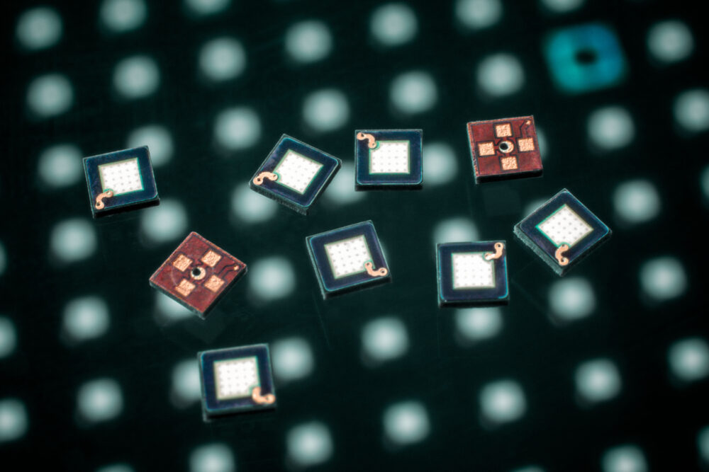
Concepts for the manufacture of micro batteries are currently the subject of considerable research attention. On the one hand, conventional electrode laminates, based on printed composite electrodes, are being manufactured in even more compact form factors and encapsulated in metal housings. On the other hand, attempts are being made to increase the still very small surface capacity of solid state thin-film batteries by 3D-structuring the electrodes. However, the processes to achieve this are complex, not very widely available, and therefore comparatively expensive.
A technology developed at Fraunhofer IZM and the TU Berlin is based on the combination of a housing and composite electrodes (based on silicon technology) that can be manufactured using standard microsystem technology processes. The composition of these electrodes has been specially adapted to the special features of microstructure deposition and can be implemented even in very small cavities. A special diffusion barrier layer prevents Li ions from diffusing into the silicon housing. The cells described achieve surface capacities of about 1 mAh/cm², with a current carrying capacities of 5 to 10 mA/cm² as well as cycle stability of several 100 cycles. They can already compete with the smallest accumulators available on the market.
It is also possible to tailor cells precisely to customer requirements: Depending on the application, the nominal voltage and the shape of the discharge curve of the battery are adapted by selecting the electrode materials. Using special technologies, it is possible to manufacture battery electrodes with a precise microstructure. In this way, the current carrying capacity and impedance behaviour of a specific battery chemistry can be specifically optimized, or the shape of the battery can be adjusted for each target application.
Successful projects: Hearing contact lens
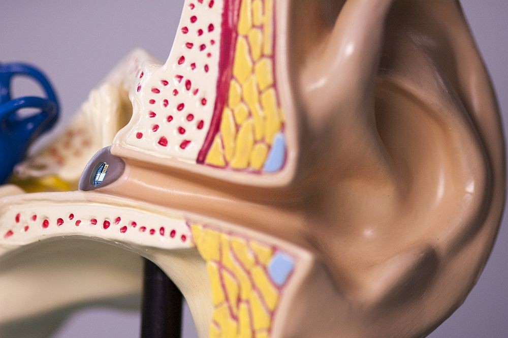
The concept has already been successfully implemented in various practical application scenarios. The BMBF-funded research project “Hearing Contact Lens” (www.hörkontaktlinse.org) is currently developing a shape-specific lithium-ion accumulator in cooperation with Auric Hörgeräte, the University Hospital of Tubingen, and the TU Berlin with its Research Center of Microperipheric Technologies. The new lithium-ion accumulator supplies an innovative, extremely miniaturized hearing aid with energy.
The hearing contact lens is attached directly to the eardrum and thus represents an intermediate form between an implantable and an external hearing aid. It is designed to provide people with mild to profound hearing loss with natural directional hearing, while offering the wearer a comfortable experience. The target for the battery is a running time of two days and a maximum charging time of 30 minutes. The overall system has a diameter of only 6 mm (Fig. 2). For applications with very low discharge currents, however, much smaller cells can be hermetically encapsulated. The first silicon-integrated micro-batteries are already available with a housing edge length of only 0.5 mm and a total thickness of 200 µm.
This article is based on the publication “Panel-Level-Packaging: Trends der Systemintegration für digitale Vernetzung” (www.all-electronics.de).