Electronic packaging stands on the cusp of a new wave of innovation, propelled by recent progress with autonomous cars and mobile consumer electronics. A group of industry leaders from Europe, the US, Japan, and Korea has assembled to put in place the fundamental processes for new panel-level packaging technologies and explore the technological limits for large-scale organic substrate formats.
There is only one place for pre-competitive R&D of this nature: Fraunhofer IZM in Berlin, where the world’s most productive consortium for panel-level packaging just took a major next step, launching the Panel Level Consortium 2.0 (PLC 2.0) with new members and exciting new research approaches.
The output of the first consortium will be picked up and spun further with the industry leaders in production technology, advanced process, materials and equipment development.
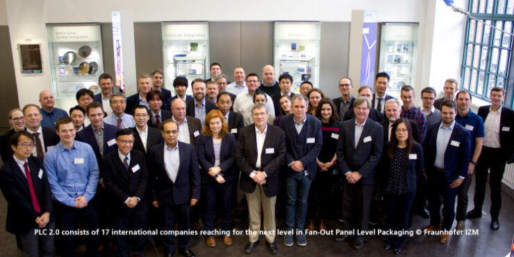
The first Panel-Level Packaging Consortium brought together 17 international partners from the industrial world in a high-powered project, spearheaded by the Fraunhofer Institute of Reliability and Microintegration IZM as a renowned expert for substrate technologies and wafer-level packaging. In its two years of hard work, the Consortium focused on the entire process chain in panel-level packaging: from assembly, molding, wiring, cost modelling, and standardization. The results of these efforts created the foundations for an innovative process that allows the production of low-cost packages on full panel formats on an industrial scale. Extremely thin packages were also developed that forego the usual substrate without compromising on their electrical properties and extraordinarily low thermal resistance. The resulting packages provide an ideal opportunity for use in high-frequency applications like 5G or radar technologies.
The success story of the first PLC: 300,000 chips, 30,000 SMDs, and 110 panels in 2 years
Already within its first year, the Consortium established and optimized the entire process chain for semi-format panels (18×12 inch). The second year was dedicated to modifying the original design and scaling the technology to full-format panels (18×24 inch) based on the first year’s findings. The Consortium also managed to integrate new vertical integration elements and passive components. On the technical side, it produced an incredible 110 panels, including 300,000 chips and 30,000 SMDs. However, the achievements were not only limited to technology: the Consortium developed an intelligible and flexible cost model to cover various types of applications and materials. The results were shared with a wide public during scientific congresses and industry exhibitions.
The success of this venture led Fraunhofer IZM to launch a second iteration, the all-new PLC 2.0, which sees actors returning from the first Consortium alongside new members. The extension of the cost model by a fine line routing model to other packaging architectures, including user-friendly software modifications, is also a target.
The project is divided into three focus thrusts. The key benefit of the first thrust is the exploitation of die placement and embedding technology for fine line wiring FOPLP. Its main goals include diverse process developments, the evaluation of materials, and the investigation of additional parameters concerning die shift and warpage. The work will include strategies for controlled warpage and process flow simulations.
The second thrust is about extreme wiring and exploiting the technology of the fine line wiring. The project aims to develop 2 μm L/S on full IZM panel size and to exploit the ‘via-less’ Chip-to-RDL interconnection. In addition, a fine line study will explore the challenges down to 1 µm L/S and below on panel formats.
Migration effects and exploiting the migration limits of fine wire line wiring are the subjects of the third project thrust.
Tanja Braun, group leader at Fraunhofer IZM, is the public face of the Panel Level Packaging Consortium and won the nickname ‘Miss Panel’ due to her extensive knowledge of panel-level packaging and the numerous publications she authored in recent years. New equipment for panel-level packaging has been installed in the run-up to the PLC 2.0. The project benefits from several major investments the German Federal Ministry of Education and Research made in the Research Fab Microelectronics Germany. Furthermore, the Consortium’s structure was simplified with a single membership category, made possible through the successful implementation of the PLC workflow.
You can process thousands of packages on a panel at the same time. Usually, it is quite a big effort to get all the components. You need to develop such a process, and it takes a lot of time. The idea of the Consortium was to share the high development costs between the partners. Each partner deposits a membership fee and in return, we share the work, the results, the equipment, and so on. Our ambition is to get closer to the physical limits.
Dr. Tanja Braun
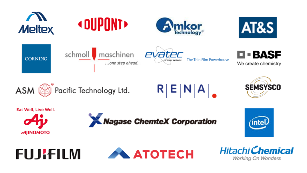
The new partners of the PLC 2.0 include:
Other companies interested in joining the Consortium still have an opportunity to do so until summer 2020. You can find more information about PLC 2.0 here.