The future of microelectronics faces exciting developments and important trends. But how will this technological sector develop in the coming years? Which application areas will significantly drive 2.5D/3D hetero-integration and high-end performance packaging, and where are the limits of what is physically possible?
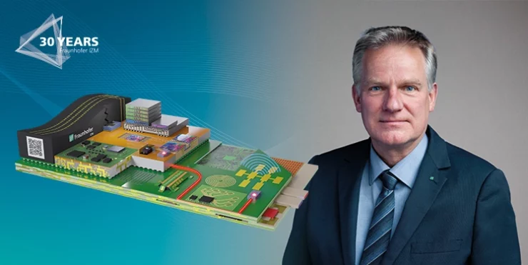
On the institute’s 30th anniversary, RealIZM, the science blog about microelectronics at Fraunhofer IZM, met with Prof. Dr. Martin Schneider-Ramelow. The institute’s director gives a comprehensive insight into the future of microelectronics as well as current and planned research activities.
How do you envision the future of microelectronics? Which important trends do you think will shape the coming years?
Prof. Dr. Martin Schneider-Ramelow: The fact is that we will not produce the logic and the memory devices with the finest structure widths within semiconductors (nodes) in Europe, even if large manufacturers like Intel or TSMC want to locate here. In this field, as we know, there are only a few large international manufacturers who have the machinery and expenditure to produce nodes smaller than 5 nm. BUT… It is becoming increasingly important to bring these devices together with other devices that have different internal structures, such as sensors, power electronics, voltage supplies, etc.
At Fraunhofer IZM, we have been researching and working on 2.5D/ 3D hetero-integration for many years. The equipment and the possibilities that our institute has for research and development in this field are unique in Europe. This has encouraged me to remain with the institute for as long as I have and to take on the role of institute director.
Some companies are already talking about 5.5D hetero-integration. This is the combination of 2.5D and 3D. In other words, chips are stacked on top of each other and electrically connected to each other, and are also connected to each other on an interposer or organic substrate on which other components as well as semiconductors or chiplets are located. In packaging, the trend is emerging to go further and further with width and height. Our Institute for Microintegration is very well positioned in this area. Our goal is to continue to play a pioneering role in this area.
Which application areas are significantly driving 2.5D/ 3D hetero-integration?
Prof. Dr. Martin Schneider-Ramelow: These are buzzwords that have been heard in the professional world for the last three to five years. The demand for high performance applications for data centers, high performance computing (HPC), quantum computing and neuromorphic computing, smart sensing, optoelectronics, 5G and 6G communications, artificial intelligence (AI) and also autonomous driving is steadily increasing.
On the one hand, AI training and inference is driving demand for data center servers. On the other, more and more supercomputers are being used to perform complex tasks such as imaging digital twins and calculations for climate research and quantum mechanics. Last but not least, cloud computing and video streaming are becoming increasingly popular.
All these applications generate an extremely large amount of data, and their processing and transmission require much better computing. With 3D hetero-integration, Fraunhofer IZM is making an important contribution to this.
If conductor paths become even narrower in the future, via diameters even smaller, wafer thicknesses even thinner – when will we reach the limit of what is physically possible?
Prof. Dr. Martin Schneider-Ramelow: Some years ago, people said that Moore’s Law would slowly put an end to fine internal structures. Some leading manufacturers have announced that they will be using nodes smaller than 5 nm in the future. Yet a few years ago, no one could have imagined this.
A new trend is also emerging for finer structures on printed circuit boards, i.e. organic substrates, which are targeting the lower single-digit micrometer range. This is not yet state-of-the-art. I am convinced that colleagues at our institute will be instrumental in advancing this field. The foundation has already been laid for achieving even smaller sizes. For one thing, we are applying new technologies such as hybrid bonding. Secondly, major research and funding measures mean we have numerous new devices at our disposal that can be used to implement even smaller structures.
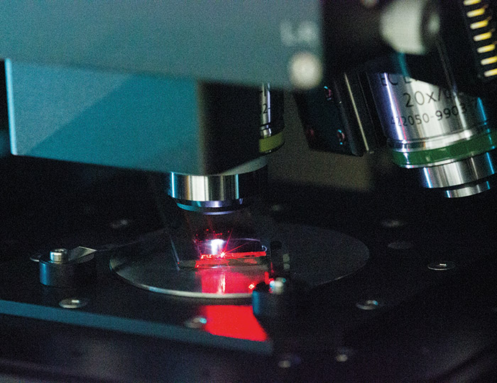
Since 2022, Fraunhofer IZM’s QuantumPackagingLab has been one of the leading centers for the development of reliable packaging approaches in quantum photonics. Our experts in optical interconnect technology, for example, have a special 3D printer for laser processing of glass with an accuracy of about 1 µm at 200 x 200 mm. To our knowledge, there are only 10 machines in use worldwide in this research area. The machine is designed for four processes: selective laser-induced etching of glass, welding of glass, writing of 3D waveguides, and two-photon polymerization. Normally, a single machine is required for each of these processes.
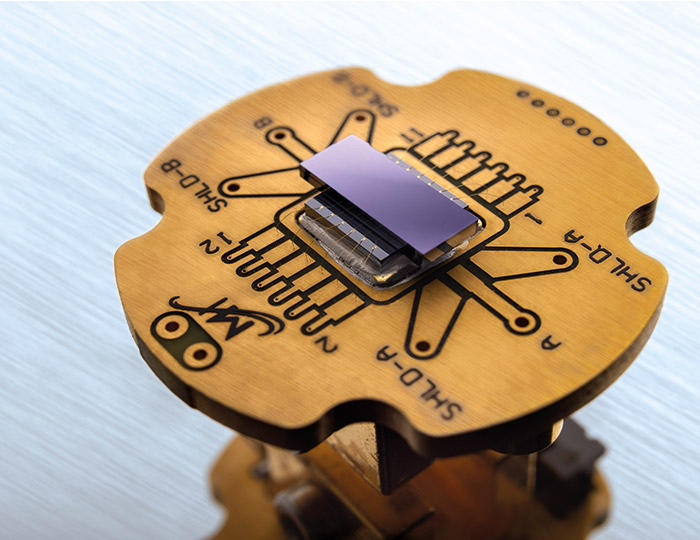
Quantum technologies and high-speed computers using superconductors are among the latest electronics trends. However, the structures with which qubits on chips, for example, can be controlled and read out in real time are still larger than the qubits themselves. A research group at our institute has recently developed a process which allows them to use indium bumps to double the connection density compared to previous solutions. They now want to use this technology to optimize the drive electronics. In addition, we have set up a cryogenics laboratory at our Berlin site, which can be used to test the performance of the electronic assemblies at temperatures of just a few Kelvin.
Left: On the way to market-ready quantum technologies: Packaging technologies for quantum photonics are being developed at the Berlin QuantumPackaging Lab. | © Fraunhofer IZM, Matthildur Valfells
Right: Chip assembly for readout electronics in quantum computers on cryo test pedestal. | © Fraunhofer IZM, Volker Mai
To return to the initial question, there will indeed be a point where we will not be able to get any smaller. Eventually, photonic data transmission, which is already used from rack to rack, will also go directly into the PCBs as well as from chip to chip. We have already been working on this for several years.
A few weeks ago, the Research Fab Microelectronics Germany (FMD) and Intel, together with key players in German industry, presented a Roadmap 2030+ for 3D integration research. What contribution will Fraunhofer IZM make to this?
Prof. Dr. Martin Schneider-Ramelow: Our institute has played an important role in initiating talks with Intel; we have been working closely together for many years. The research roadmap just presented was developed in a series of workshops organized by FMD and Intel Europe Research. The first workshop took place at our premises in Berlin at Fraunhofer IZM.
A historic meeting at our institute, marking the beginning of an extraordinary partnership: The first FMD-Intel Workshop on Heterogeneous 3D Integration for 2030+ on October 28, 2022 in Berlin. | © Fraunhofer IZM
We have also been actively involved in the development of the roadmap and are preparing the foundations for future microelectronics together with the relevant stakeholders. It is of great strategic importance that Europe as a location does not fall behind and that future developments are promoted and advanced in close cooperation with industrial partners. Chiplets have been talked about for many years. However, only small quantities are in production worldwide. We are still a long way from supplying finished chiplet solutions, but there is a roadmap for implementation in the coming years in place. In the future, nodes with extremely fine structures will have to be combined with sensors, MEMs, photonic elements, LiDAR, radar, and much more for use in the automotive sector. The resulting data volumes must be processed. At Fraunhofer IZM, we are convinced that this will only be possible in the future with chiplets. The semiconductors and components from the various Fabs and from the Fraunhofer Institutes or other European research and technology organizations (RTOs) must be very tightly interconnected in the smallest possible space. Technologies such as our panel level packaging play an important role in this context. The fact is, in the end everything has to be integrated onto a substrate to connect the chiplets with the other components. Before mass production can start, key questions need to be answered: Who are the potential customers for these components? What opportunities are there for cooperation with industry in Germany and Europe?
The current institute brochure shows a visualization of a High-End Performance Package (HEPP). What does this illustration show and what exactly constitutes a HEPP?
Prof. Dr. Martin Schneider-Ramelow: The graphic visualizes how crazy systems get when they are supposed to be highly functional and what technologies are needed to achieve this. We illustrate what is already being done today in high-end performance packaging and where our institute is active in the field of hetero-integration. We put chips on and into the printed circuit board. We build interposers, stack chips and process MEMS in systems. We take care of cooling, antennas and data transmission. Fraunhofer IZM is the packaging institute in Germany, Europe and worldwide.
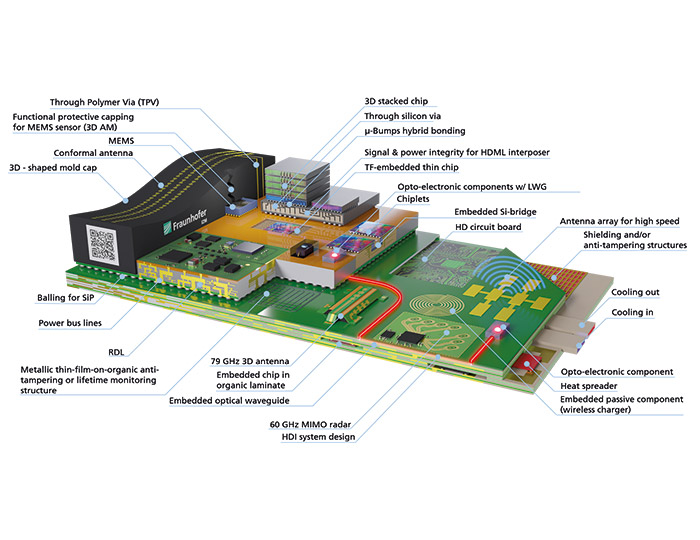
High-End Performance Packaging from wafer to system | © Fraunhofer IZM
The current challenge is that the industry is setting new standards in terms of finer structures, micro-bumps, fine lines and spaces. To keep up with this and deliver innovations ourselves, we need the latest machines and measurement techniques. We contribute by developing and building systems that the industry can then produce. Whilst we look at the overall concept, companies focus on specific areas of development, e.g. packaging, chip design development and the production of chips, MEMS, or sensors. However, in the end, a functional system must be created from these individual building blocks.
We see ourselves as a link between the manufacturers of the materials, machines, components and the specialists in packaging and interconnection technology. As an application-oriented research institute, our approach is to understand what the respective application requires in terms of technologies, components, materials and reliability. We are at the center of all activities in the preparations for the European Chips Act (ECA).
Hybrid bonding and chiplet integration are increasingly being mentioned in connection with advanced packaging. However, new approaches must be taken for packaging modern power semiconductors such as silicon carbide (SiC) or gallium nitride (GaN). How is Fraunhofer IZM positioned in this respect?
Prof. Dr. Martin Schneider-Ramelow: As explained earlier, the microelectronics industry has been increasingly focusing on heterogeneous integration for several years in order to integrate more computing, memory and other functions on a given area. To increase 3D interconnect density, multiple advanced and/or mature chips are being placed in a single package. However, for high-performance applications, the IO spacing requirement shrinks below what can be achieved with flip-chip interconnects. To reliably interconnect chips with a pitch of 10 µm, hybrid bonding technology is currently the only option.
We have been working on hybrid bonding in industrial projects at our site in Saxony for several years. So far, we have been working with bonding widths of 4.5 – 6 micrometers. We need to collaborate to reduce that by half, as we do not yet have the necessary machinery. However, we are planning to acquire the necessary equipment through funding programs (including the ECA). We know how and under what conditions this works in a clean room. There is still a lot of development to be done for the expected sub-micrometer structures by the end of this decade.
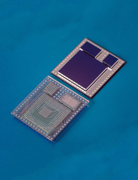
Left: Silicon interposer with two assembled Risk-V-based chiplets and two high bandwidth memory stacks (HBM2) for high performance computing and AI workloads. Chip/system design: ETH Zurich, interposer finish and chip assembly: Fraunhofer IZM. © Fraunhofer IZM
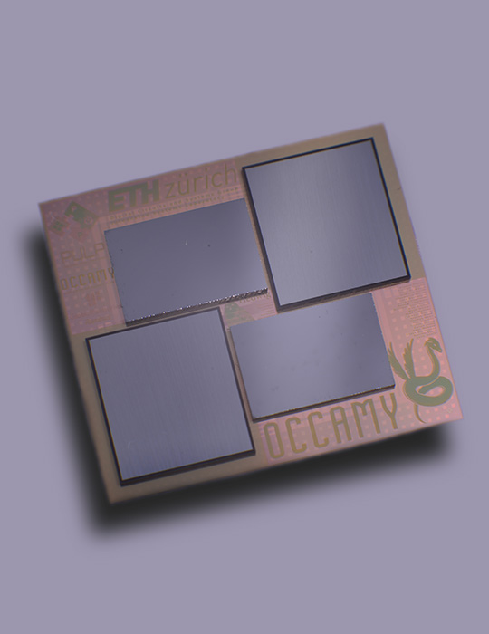
Right: Glass interposer with 3 assembled daisy chain test chips. The thickness of the glass interposer 450 µm with completely Cu-filled TGVs and RDL routing on both sides. Glass can offer a superior performance for RF applications (depending on glass type) and can be processed to an interposer with thicknesses in the range of 50-800 µm, TGVs can be used for power or signal routing or to improve thermal management. © Fraunhofer IZM
We also play a pioneering role in the field of chiplets. We work on both silicon and glass interposers and are also exploring the possibility of working on organic substrates. Over the next few years, it is expected that the internal chip structures for some types of semiconductors will drop to a size range of less than 2 nm. As far as the bonding of these chips on substrates is concerned, the first IC substrates with two micrometer lines and spaces (L/S) are already in use in Asia. However, there are still a number of technical questions to be answered here, e.g. whether the high-frequency capability and signal integrity are guaranteed, and how does heat dissipation of the system take place? These are also the challenges that motivate me personally.
It is important to understand that Fraunhofer IZM does not manufacture semiconductors, i.e. we are not a CMOS institute that designs and manufactures chips. We start with the wafer. But if, in the future, the external connections of the chips and other components are also to become smaller and smaller and are to be placed as a system on an organic, glass-based, or ceramic substrate or even embedded in the printed circuit board, there will be some development work required. This is where Fraunhofer IZM comes into play. Our two main technologies are wafer level packaging and (large area) substrate system integration, both of which are being stringently developed.
Using printed circuit board technology, we have embedded power semiconductors partly with ceramic interposers to realize high-performance power electronics. For this purpose, we build subsystems, modules, and systems and also take care of the packaging and cooling. For many years, our institute has been involved in pre-development on future topics at ECPE, the European Competence Center for Power Electronics.
I am certain that we will make significant contributions to microelectronics in the future. One thing is for sure, we will not run out of research topics in the next 30 years.
What ideas and plans are there for the future design of Fraunhofer IZM’s three sites in Berlin, Dresden and Cottbus?
Prof. Dr. Martin Schneider-Ramelow: The Innovation Campus for Electronics and Microsensors Cottbus – iCampµs Cottbus – was established in 2019 with six non-university research institutions as well as professors from BTU Cottbus-Senftenberg. Our institute is involved in various projects in the field of high-frequency and high-speed systems and antenna configurations. One example project is the development of a mobile ultra-low power radar system for medical applications. I am very pleased that we are also represented with a professorship in the field of high frequency technology at iCampµs Cottbus since the beginning of 2023.
Next year, the iCampµs Cottbus Conference (iCCC2024) will take place, to which I cordially invite everyone from research and industry. The transfer conference for innovations in science and industry will highlight potentials and new applications arising from powerful sensor technology, the use of innovative microelectronics and AI for Industry 4.0, the energy industry and (tele)medicine.
I have high hopes to expand Fraunhofer IZM-ASSID at our Dresden site in the long term. Unlike Berlin, the site in Moritzburg is owned by the Fraunhofer Gesellschaft. This means that we have the opportunity there – provided we have the funds available (in the lower three-digit million Euro range) – to double the existing cleanroom area and equip it with the appropriate machinery.
For Germany, it would be great if Fraunhofer IZM-ASSID had its own manufacturing capacity. I believe we could supply sophisticated modules, submodules, small systems and preliminary products in the future. I am happy to support this path, we just need the financial resources and also the demand from industry. However, this is still all pie in the sky.
Another option is to rent existing or planned clean rooms. Together with the Fraunhofer IPMS, we have found a solution for this at the Centers Nanoelectronic Technologies (CNT) in Dresden. In summer 2022, the new cleanrooms at the CNT and the 300mm Center for Advanced CMOS & Heterointegration in Dresden-Moritzburg were opened together with the IPMS. Over the next five years, we plan to create additional cleanroom capacity of up to 900 m2 and equip it with a pool of equipment to work together with the Fraunhofer IPMS and CNT. We need to have access to the latest machines and plan cleanroom capacities in this regard in order to keep up with developments in high-end performance packaging. We therefore cooperate with numerous partners – machine, material, user and packaging specialists. Various support measures and our cleanrooms mean we have been very successful in this so far. Our location in Berlin is currently benefiting in particular from funding from the German Federal Ministry of Education and Research (BMBF) for the “Research Factory for Quantum and Neuromorphic Computing” (FMD-QNC) project. The existing premises are continuously optimized and modernized and technologies are further developed.
In addition to the term microintegration, Fraunhofer IZM has the term reliability in its name. Where should reliability assessments ideally start?
Prof. Dr. Martin Schneider-Ramelow: The reliability of electronics is the basis for functioning systems. At Fraunhofer IZM, we look at high-end performance packaging, i.e. heterosystem integration, in terms of materials, components, and machines as well as assembly and interconnection technologies, testing, characterization, and reliability, all the way to the application as a whole. We are therefore particularly strong in physics-of-failure analysis. This means that when we build new systems with new materials and finer structures, we know which stresses are to be expected depending on the area of application. This allows us to reliably align and simulate electronic systems in a targeted manner. We are interested in then applying the simulation to the new technologies we develop and new materials we use. Not only do we do the reliability testing and analysis, but based on that we describe the failure and failure mechanism. What is the use of building a system that is defective in application after two days?
The evaluation of reliability must be carried out at coordinated technology levels and requires an understanding of the respective system. Where, how and when is the component installed and to which stress factors (temperature level and change, humidity stress, load duration, etc.) is it exposed? Reliability measurements should be taken as early as possible in the process. The need for technology-accompanying reliability analysis will play an increasingly important role in the topic of chips. If chips from different manufacturers and technologies are installed in a multi-package, in the worst case a “bad” chip or an inadequate interconnect is enough to cause the entire system to fail.
After all the insights, you get the feeling that these are golden times for microelectronics. Is that really the case, or are there also challenges?
Prof. Dr. Martin Schneider-Ramelow: The need to constantly renew machinery and to maintain and operate cleanroom infrastructure are cost-intensive. There is also a shortage of skilled workers. At the Berlin site, we currently have over 100 laboratories across a total area of 8,000 m2. In order to staff all of these, we need aspiring scientists and technicians. We have been training future microtechnologists for over 20 years. Our research institute offers exciting tasks and perspectives for further development, for students and even more so graduates.
Sovereignty is currently a key topic in the industry. In order to be able to provide essential advance developments for industry, research institutes need the financial resources to build and operate an appropriate technical infrastructure. My appeal to our headquarters in Munich and also to the decision-makers in politics is as follows: Continuous investment in the education and training of specialists for microelectronics and in equipping the research institutes is worthwhile and will continue to be necessary. We have already achieved a great deal. As a result of the European Chips Act (ECA) and numerous initiatives such as FMD funding by the BMBF and the above-mentioned “FMD-QNC”, I am observing increasing networking with European research organizations such as imec and CEA-Leti. It is only together that we can develop solutions for the current and future challenges in electronics research.
Despite all the euphoria about technology, it is also important to consider the impact of newly developed technologies on the environment and their energy efficiency. The fact is that more and more electronics are being installed. If medical operations are performed in the future with the support of a digital twin, or if vehicles drive autonomously, this will also mean higher energy requirements. Operating new electronic products at the lowest possible energy level, thinking about their recycling through to reparability, are becoming increasingly important in electronics and packaging technology.
Fraunhofer IZM has been concerned with the impact of technological progress on the ecological footprint since its foundation. We have been the absolute pioneer in this field for 30 years in the international research community. In the early days of our institute, we discussed the topic of “lead-free electronics” thoroughly and have continued to work on the issue of electronics-specific sustainability ever since. Our work in this area is currently culminating in the “Green ICT @ FMD” project. In this, we are looking at how sustainable electronics can be. For example, we are looking at the material cycles and carbon footprint of electronics in all the areas that are used in high-end performance packaging. Our job is to take a holistic view of what we develop and build in high-end performance packaging. It’s not enough to have the most innovative packaging process. We also have to make sure that the technologies we use work reliably and are sustainable at the same time.