
Welcome to our list of the IZM´s breakthrough technologies. In this post, you can learn about the four hallmark technologies in the field of microelectronics developed by Fraunhofer IZM that have the greatest potential or are already in widespread use around the world.
1. The first application of wafer-level packaged chipsets in a medical device (pacemaker)
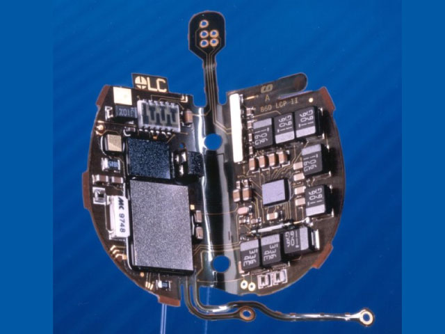
© Fraunhofer IZM
One of the most interesting breakthrough research projects was a development of a novel generation of pacemakers. This was achieved in a 1997-1998 project completed together with the TU Berlin and Biotronik, the largest manufacturer of pacemakers in Europe.
The biggest challenge for IZM was the choice of an innovative wafer-level packaging technology for the development of highly miniaturized, light, and reliable packages for pacemakers that added greater functionality while reducing manufacturing costs. Fraunhofer IZM was the first institute working with this technology in Germany. For this project, a wafer-level chip size package was developed and installed on a rigid-flex-FR4 circuit board instead of a ceramic board. The use of WLP for medical application was another novelty, as the reliability requirements of packages in harsh biological conditions are very high. Today, WLP are the most common packaging solution for portable electronic products like smartphones.
Through this project, Fraunhofer IZM and our partner created a new technology for the medical industry that is still in mass production today.
2. World´s smallest camera
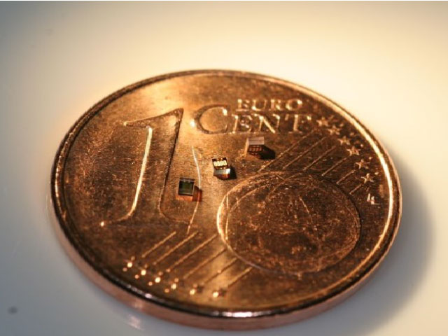
© Awaiba GmbH
In a partnership with Awaiba GmbH on the BMBF research project “ComiKa”, Fraunhofer IZM has developed an image sensor package for medical applications (such as endoscopy). The main idea was to combine wafer-level glass optics with the 3D integration of a CMOS image sensor. The developed image sensor package was miniscule not only in size alone, but also in terms of costs: More than 22000 cameras are packaged in a single step on a 200 mm wafer. To achieve this, Fraunhofer IZM used a backside contacting of the CMOS wafer for the very first time, employing through-silicon vias (TSV) for the sensors. For this technology, the CMOS wafer is glued to a glass wafer and then thinned down to a few tens of microns in thickness. The idea of the glass wafer was to thin the sensor wafer and to protect the sensor surface. After realizing the TSVs and subsequent backside rewiring, the optics and image sensor were integrated using wafer bonding. Depending on the chosen application, several wafers holding the lenses and spacers were glued together with high lateral accuracy (with an offset of
Based on the R&D work of the cooperation partners, a prototype of a micro-camera was developed for use in disposable endoscopes, achieving a resolution of 62,500 at a total size of less than 1.0 mm x 1.0 mm x 1.0 mm.
3. Pioneering development of a 5G antenna
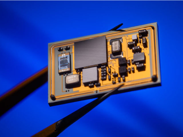
© Fraunhofer IZM
Fraunhofer IZM teamed up with nine industry and academic partners as part of the European Serena research project to develop a low-cost, high-power, and high-efficiency RF platform for next-generation 5G communication and new radar systems for autonomous cars. Fraunhofer IZM provided the HF design and the fabrication and testing of the system integration platform for mm-wave systems. The 5G antennas not only had to achieve high gain, but also a wide broadband that provides a very high data rates in the frequency range up to 38 GHz. Both of these characteristics rely on the materials (substrates) used to build the antennas. The biggest challenge in making this possible was the 28-35GHz package design for 5G modules with integrated antennas, which needed to use new materials in novel combinations.
The main research idea consisted of a semiconductor technology using cost-efficient gallium nitride on silicon (GaN-on-Si) (achieving unprecedented efficiency and output an order of magnitude greater than silicon germanium (SiGe)) and heterogeneous casing designs. A key objective was to obtain an energy-efficient technological solution to reduce the size and costs of systems while increasing transmission power and capacity.
4. Best-in-Class Supplier for the ATLAS Detector in CERN’s Large Hadron Collider

© Fraunhofer IZM
Another breakthrough solution that Fraunhofer IZM contributed together with scientists from TU Berlin was a development of detectors for the CERN Particle Accelerator. Approximately 1,700 detector modules were manufactured for the Large Hadron Collider, covering 2 m2 of the inner wall at the collision site and detecting the energy of elementary particles. With every single detector sensor having a resolution of more than 46,000 pixels, the system has become the largest digital camera in the world.
One of the greatest challenges was the development of a high-density interconnect approach for the particle detection modules. Because the particle packages hit the detector every 25 nanoseconds, all pixels have to be detected at a rapid 40 MHz, which requires a huge number of read cables. Thanks to our scientists, we achieved 40-µm chip interconnection, far ahead of the state of the art at the time of its development. This was made possible by using high-density flip-chip technology that reduced the size of the components and shortened the signal paths to a minimum. The design also allows for better electrical, mechanical, and thermal contact.
Since 2000, Fraunhofer IZM has been supplying most of the particle detection systems around the world.
IT CAN BE ALSO INTERESTING FOR YOU:
- Is Heterogeneous Integration a Panacea For the Electronics Industry?
- Will Chiplets Revive Moor’s Law?
- How Waterproof Flexible LED Systems Became a Reality
