Finding a way to make the production of thermal infrared sensors cheaper would open up numerous new possibilities for thermal imaging systems e.g. for automotive and security applications. This is why Fraunhofer IZM researchers have been working on wafer-level packaging processes specifically for the hermetic encapsulation of large MEMS pixel arrays in a vacuum. On top of everything, the robust manufacturing process can make production up to 100 times faster.
RealIZM has met Dr. Charles-Alix Manier, development engineer at Fraunhofer IZM, to speak about the EU research project APPLAUSE, the great potential of packaging technology and how Wafer-level packaging processes can be used for low-cost infrared cameras.
Can you tell us what was behind your work on refining the wafer-level packaging processes?
Dr. Charles-Alix Manier: Our research institute was part of a European consortium that participated in the EU project APPLAUSE, which stands for “Advanced packaging for photonics, optics, and electronics for low-cost manufacturing in Europe”. The aim of the project was to develop new packaging and interconnection technologies for highly integrated microelectronic and optoelectronic systems to be manufactured in Europe in a commercially competitive manner.
Fraunhofer IZM was involved in the development of three use cases. One of them was to develop a low-cost infrared camera with increased video rates and VGA resolution for automotive and security applications using a microbolometer-based sensor. Microbolometers are used as infrared image sensors in thermal imaging cameras.
What does a microbolometer look like?
Dr. Charles-Alix Manier: The heart of the thermal imaging camera is an integrated image sensor chip (or focal plane array) consisting of readout electronics with tiny MEMS cells, arranged in a matrix of 20,000 up to 1 million pixels. Each pixel consists of a small microbolometer, in this case arrayed in a 17 µm pitch and with a resolution of 640 x 480 px per array. Microbolometers are thermal sensors that convert thermal radiation into electrical signals and measure electromagnetic radiation like infrared in the long-wave infrared range between 8 and 14 µm (LWIR).
Technical specifications:
17 µm | Pixel spacing between the individual microbolometers |
640 x 480 px | VGA resolution/arrangement of microbolometers in an array |
12,3 x 11,2 mm2 | Side dimensions of the caps |
13,6 x 13,1 mm2 | Size of the microbolometer die incl. all peripheral circuits and IO-pads |
Microbolometers are based on a thermally insulated membrane consisting of a heat absorber layer. When that layer’s temperature changes, its electrical resistance changes as well. So for microbolometers to work properly and be sensitive enough, they need to be thermally insulated, which means that they need a vacuum environment that prevents any heat loss by convection. For this purpose, the MEMS structures are covered with a cap that not only protects them mechanically and keeps them clean and free from dirt, but also maintains the vacuum and a hermetic seal against the ambient air. At the same time, the cap must be transparent in the LWIR range to allow as much of the radiation as possible to reach the microbolometers.
The microbolometer array’s capping, the vacuum under its caps, and any changes in the vacuum over time affect the reliability and performance of infrared sensors. Our mission was to develop robust wafer-level packaging processes that can produce thermal infrared sensors at high volumes, but at lower costs.
How does your wafer-level packaging process hold up, compared to existing manufacturing processes?
Dr. Charles-Alix Manier: Our concept is based on making large cap structures on temporary carrier wafers and metallic bond frames. The caps are then soldered to the device wafers via metallic double-sided bond rings, and all under vacuum.
The special feature is that all chips on the device wafer are hermetically sealed in one go, instead of individually. The current industry standard in infrared sensor manufacturing uses chip-to-chip packaging. This process requires a large number of individual steps and is more time-consuming and cost-intensive than wafer-level packaging.
»With our approach, we can speed up the manufacturing process of thermal infrared sensors roughly by a factor of 100, assuming that a 200 mm wafer can hold from approximately 100 up to 250 chips, depending on chip size, resolution, and MEMS pitch. In addition, we achieved a tight seal for over 95% of the chips on the wafer. For outsiders, this may only be a small step forward, but for us scientists and European electronics research as a whole, it is an significant R&D milestone.«
Dr. Charles-Alix Manier, Development Engineer, Fraunhofer IZM
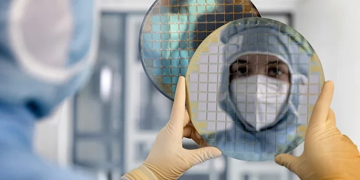
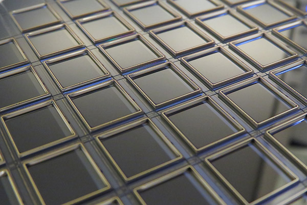
MEMS-based infrared image sensor chip encapsulated in a vacuum on a 200 mm wafer | © Fraunhofer IZM
To determine the quality of the sealing, we used a number of so-called Pirani vacuum test structures. First, resistance to pressure was measured in a controlled vacuum and then compared with the identical structures after encapsulation. This allowed us to determine the residual vacuum inside the caps.
The hermetic encapsulation under vacuum further protects the highly sensitive MEMS permanently during all later integration processes, up to their integration in the final camera sensor. At the same time, they stay fully operational, and infrared radiation can pass through them.
Can you tell us more about how hermetic capping is done in a vacuum?
Dr. Charles-Alix Manier: The wafer-level sealing process we use is based on AuSn soldering in vacuum. To bond the cap structures, bond ring structures are prepared first, in our case using Au rings (metal frames) as the bonding interface for all cap structures. This requires complementary rings of Au+Sn on the counterpart (device wafer) to make it possible to solder the caps on.
All device wafers must undergo electrodeposition to form the Au+Sn rings. In our project, this was done with a semi-additive process, which includes sputtering a seed layer, lithography, electroplating, removing the resist, and etching the seed layer.
All of these processes affect the surface of the wafer and cannot be applied to wafers with free-standing bolometers. These are thin and extremely fragile once they are released from the so-called sacrificial layer holding them initially.
We succeeded in moving bolometer release to the end of the manufacturing process – just before bonding the wafers, keeping the bolometers intact. This allowed us to perform the semi-additive process before the sacrificial layer is removed – that is, before the microbolometers are freestanding and in consequence fragile.
After both wafers are aligned using dedicated marks, the AuSn wafer bonding sequence is performed. In this step, the AuSn ring melts and wets the Au counterpart. A transient eutectic (liquid phase) forms over the Au frame, which undergoes a reaction and solidifies at the latest during cooling. The AuSn frame can no longer melt after bonding due to phase transformation in the metallic bond. The resulting alloy is stable up to about 500° degrees.
After bonding the caps to the wafer, their temporary carrier bond on the back is released by laser-assisted debonding. As a result, the caps remain on the device wafer and all other structures on the carrier wafer. This so-called “selective capping” covers only the MEMS field. The pad ring of the die, e.g. the input-output pads, remains thereby accessible.
Did you try other means to create the cap structures?
Dr. Charles-Alix Manier: That’s right, we investigated two different approaches that would be suitable for producing large quantities of thermal infrared sensors.
First, we fabricated monolithic caps with a deep cavity by deep reactive ion etching, using 200 mm silicon wafers with high infrared transmission in the LWIR range. The silicon wafers were also coated with an anti-reflective coating.
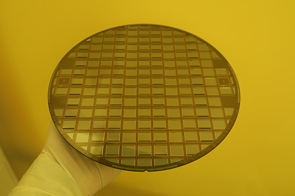
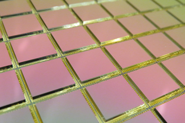
Carrier wafer with monolithic caps (left) and hybrid caps (right) consisting of silicon frame with flat silicon cap joined over AuSn bond before bonding on the target wafer | © Fraunhofer IZM
For our second approach, we developed hybrid caps to maximize internal volumes. These consist of a silicon frame (etched-through cavity) with a flat silicon cap, which are joined together via metallic AuSn bonding rings.
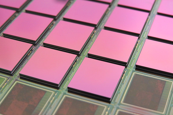
Monolithic silicon caps (left) and hybrid caps (right) tightly bonded to device wafers |
© Fraunhofer IZM
Publications:
Zoschke K., Manier C. A., Oppermann H., & Other (2023): Wafer Level Capping Technology for Vacuum Packaging of Microbolometers, vorgestellt auf der ECTC 2023, Orlando/USA