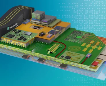
RealIZM blog series »Microelectronic Trends« – Part 2
With the newly founded Chiplet Center of Excellence (CCoE) in Dresden, Fraunhofer IIS/EAS, Fraunhofer IZM and Fraunhofer ENAS want to set new standards for automotive electronics. Dr. Michael Schiffer, head of the »Wafer Level System Integration« department, and Dr. Andreas Ostmann, head of the »System Integration and Interconnection Technologies« department, spoke to RealIZM about the need to develop innovative chiplet solutions and to drive forward heterogeneous integration and electronic packaging in Europe.
To begin with, can you please explain what chiplets are?
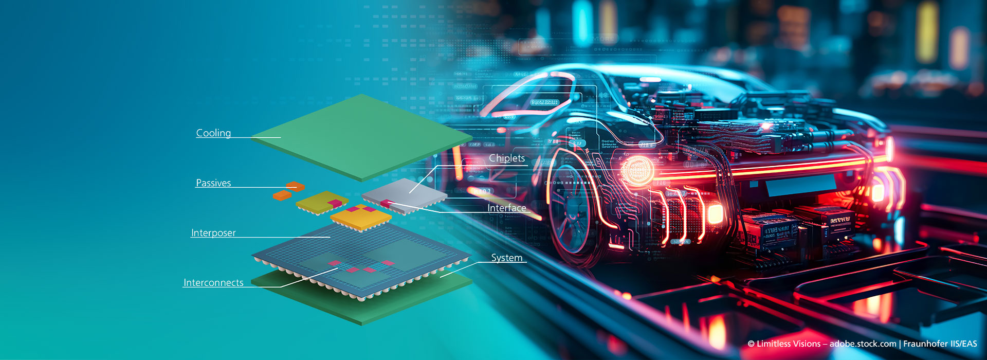
Dr. Michael Schiffer: »Chiplets« are first and foremost a design philosophy. The architecture of chiplets is based on the concept of combining electronic components of different sizes and functions both next to and on top of each other – not unlike how Lego bricks work. Wafer-thin wires serve as connecting elements. As a result, the chip components form a functional overall system – a so-called »system-on-chip« (SoC). In contrast to a »multi-chip module«, in which the various chips also function independently, a single chiplet is only partially functional in itself.
There is no standard definition for »chiplets«. Researchers typically distinguish between two approaches:
1. Individual IP blocks of an SoC are broken down, inserted as individual chiplets into a heterointegrated system, and the individual blocks are made to communicate with each other.
2. Two SoCs from different manufacturers are connected to each other via a bridge to form a chiplet system.
What are the advantages and challenges that come with developing chiplet systems?
Dr. Michael Schiffer: The chiplet approach, for example, offers major advantages in terms of hardware security and trustworthy electronics. Only the person responsible for the design of the entire chiplet system gets to access all components. A person trying to forge the system could only ever copy single chiplets in the distributed supply chain. This makes it more difficult for outsiders to copy the entire system. Going forward, other security features could be added by photonic subcomponents.
Dr. Andreas Ostmann: Creating chiplet systems is very demanding. The components must be electrically coupled so perfectly that they behave like a single silicon chip. The challenge for us as technologists is to ensure short and fast connections with as little loss as possible between the electrical components.
In your opinion, which connection technology is best suited for chiplets?
Dr. Andreas Ostmann: Flip-chip assembly is currently the most common choice for chiplet systems. For AI systems that need massive computing power, however, there is already a 3D assembly in which the individual chiplets are stacked directly on top of each other.
Chiplets have great potential for the semiconductor industry. Which applications are they already being used in?
Dr. Michael Schiffer: Chiplets are already used in the servers in large data centers that process huge amounts of data. However, the costs per chiplet subsystem for servers tend to range in the five digits. In addition, these are closed ecosystems, developed by large companies (AMD, Intel, Nvidia, Apple and Google). Only these large companies can afford to develop architectures with proprietary technologies.
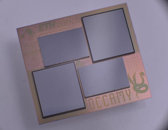
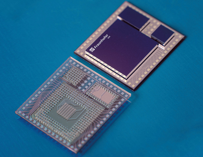
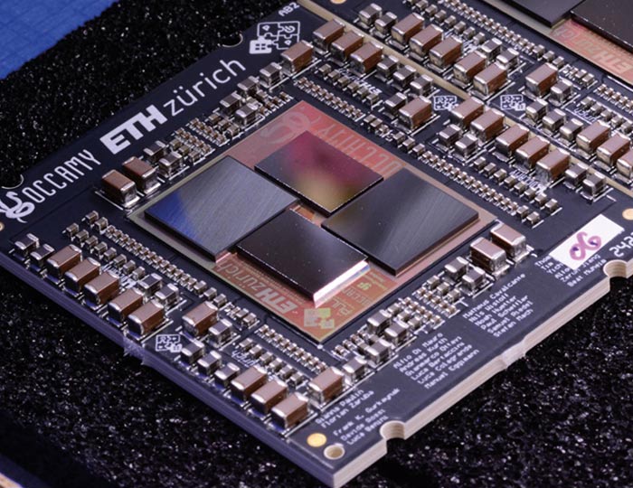
Left: Si-Interposer with two accelerator compute units and two high bandwidth memory (HBM) stacks for high performance computing. Chip and system design: ETH Zurich. Interposer finish and chip assembly: Fraunhofer IZM. | © ETA Zürich | Fraunhofer IZM
Center: Glass interposer with TGVs and assembled test chiplets | © Fraunhofer IZM
Right: AI chip with high bandwidth memory mounted on an Si interposer and carrier circuit board | © Fraunhofer IZM
Can you tell us more about the Chiplet Center of Excellence (CCoE), which Fraunhofer IZM initiated together with other Fraunhofer Institutes? What applications does it focus on?
Dr. Michael Schiffer: Fraunhofer IZM, specifically our Fraunhofer IZM-ASSID site in Dresden, teamed up with Fraunhofer IIS/EAS and Fraunhofer ENAS for a pioneering research initiative. The Chiplet Center of Excellence (CCoE) focuses on applications in automotive electronics. We cover and analyze the entire design flow, from system simulation to working demonstrators, to pinpoint any gaps.
Dr. Andreas Ostmann: One aim is to evaluate various chiplet solutions in terms of their performance, cost, and reliability. At the same time, we also see this as a great opportunity to give our R&D work in heterogeneous integration and electronic packaging in Europe a push forward.
What practical advantages do chiplet systems offer car manufacturers compared to conventional microchip systems?
Dr. Michael Schiffer: In my view, there are three reasons that make chiplet systems suitable for the automotive industry. First, the complexity of electronic systems for autonomous driving requires extremely high computing power. Second, distributed supply chains are already established in this industry. This means that the central control chip, which connects everything together, will most likely come from the respective car manufacturer.
And third, the development of chiplet systems is a cost-driven venture. To be competitive, it must be affordable. The design costs for a 7 nm chip currently amount to around 300 million US dollars. Developing a complete system can cost up to 500 million US dollars or more, depending on the number of chiplets. No single company can afford this investment.
According to a forecast by the Indian market research institute Prudour, the European chiplet market is expected to grow from USD 0.697 billion (2023) to USD 54.612 billion in 2033. The compound annual growth rate (CAGR) is 50.3% in the forecast period.
The automotive sector in particular will be driving the market’s expansion. Advanced driver assistance systems (ADAS), electric vehicles (EVs), and technologies for connected cars require powerful and energy-efficient semiconductor solutions. According to the European Association of Automotive Suppliers (CLEPA), the automotive sector is responsible for 37% of total demand for semiconductors in Europe.1
Does this mean that standards are important for the future of chiplet technology?
Dr. Andreas Ostmann: In order to be able to realize the vision of a Lego-like construction kit for chiplets, like we mentioned at the start, standards will be required in the medium to long term. There are consortia working on this standardization, such as Universal Chiplet Interconnect Express (UCIe) and Bunch of Wires (BoW).
Dr. Michael Schiffer: There is a great need for open standard solutions and interfaces that enable different chips to communicate with each other. With our expertise in assembly and connection technology, the CCoE will set innovative standards for chiplet solutions for the automotive industry.
How can the Chiplet Center of Excellence (CCoE) contribute to the development of open standard solutions for chiplet systems?
Dr. Andreas Ostmann: To put it bluntly, we are looking beyond the chip edge to enable interoperability on the chiplet market. In the automotive sector, the fact that redundancy lines will also be required for interoperability makes things even more difficult.
Dr. Michael Schiffer: At the CCoE, we see great added value in working closely with designers. Initially, we focus on technological, design support, and metrological topics. We have a variety of designs at both PCB and wafer level which are then measured by Fraunhofer IIS/EAS. Our long-term vision is to establish verified design rules for the package for the connections between the chips. One goal of the CCoE is to develop a package assembly design kit (PADK) in order to implement it in a design environment.
Which target groups is the CCoE service aimed at?
Dr. Andreas Ostmann: The CCoE is meant for automotive manufacturers (OEMs) and their suppliers (Tier 1), chip manufacturers, and semiconductor producers as well as design software developers (EDA tools). In the first step, we test the design environment. This is extremely important in order to simulate, develop, and design everything from the semiconductor to the last connections at the bottom, the bumps and interfaces to the outside world in one go.
What other expertise does Fraunhofer IZM bring to the CCoE?
Dr. Andreas Ostmann: Fraunhofer IZM supports companies in setting up affordable chiplet systems and identifying the right connection technology, system and data transmission between the individual elements for each application. To return to our metaphor of the Lego bricks: We develop the connectors – the studs.
Hetero-integration gives us greater flexibility and scalability in semiconductor design. The flexible approach allows us to develop prototypes quickly and follow iterative design processes, which in turn enables our customers to get to market faster. We develop custom solutions with the aim of getting the best performance and cost out of each application and transfer our technology knowledge to the industry. This is one of the basic ideas of Fraunhofer. We see ourselves as enablers at the system level and support new ideas for chiplet systems.
Dr. Michael Schiffer: As experts in interfaces, we offer a wide range of technological solutions – from high-end technologies such as hybrid bonding at Fraunhofer IZM-ASSID in Dresden to wafer-based solutions with interconnects with ultra-fine pitches in the lower µm range and more cost-effective approaches at the substrate level. Thanks to our large technology portfolio, we can mix and match electronic components of different functions, sizes, and process technologies when building chiplet systems. From silicon to the board, we have the expertise in-house, which is unique to Fraunhofer.
Which factor significantly influences the selection of components?
Dr. Michael Schiffer: The costs for a chiplet system in the automotive sector must be in the lower double-digit range per package. Interposers made of silicon would therefore not be the right choice. We need to check where high performance is actually required and which technology can be used to implement this in a cost-optimized way.
How does Fraunhofer IZM assess in advance how likely it is that an element of a chiplet system fails?
Dr. Michael Schiffer: We use a digital image to compare the thermo-mechanical analyses with reality. This means that we use simulations to reproduce the process flow in a digital twin in order to answer questions such as: Where do thermo-mechanical stress peaks occur that can lead to the failure of the assembly? How can we avoid or reduce these? How can the process be optimized to achieve the highest possible yield?
Dr. Andreas Ostmann: The digital twin enables us to predict what can happen if we reduce the size of the contacts or increase the distance, vary the layer thickness, or use a new, softer material. We can model the processes in the digital architecture without having to recreate them in reality, allowing us to identify errors at an early stage and get the best out of them.
Could you tell us about a real project to show how Fraunhofer IZM contributes to the development of chiplet solutions?
Dr. Michael Schiffer: In the STXMOD project, for example, we are working with partners to develop an energy-efficient stencil processor that is used together with a high bandwidth memory (HBM) on a silicon interposer for high-performance computing applications. Calculating climate models, for example, requires computing power in the exascale range. In order to perform such complex calculations, special computing architectures with fast memory modules, processors, and high-speed data buses are required.
Dr. Andreas Ostmann: We are also involved in other projects, such as the two BMBF projects CeCas and T4T. Our colleagues at Fraunhofer IZM-ASSID are supporting the T4T project »Distributed Manufacturing for Novel and Trustworthy Electronics« in the production of a 300 mm wafer-to-wafer demonstrator with an encrypted memory element and an interposer wafer with integrated chiplets.
We spoke a lot about the automotive industry. Are there other applications where chiplet systems will be used in the future?
Dr. Andreas Ostmann: The demand for powerful AI systems, machine learning (ML) applications, the increasing spread of devices for the Internet of Things (IoT), and 5G technologies are driving market expansion. Market research institutes such as Prudour also point to the switch to 5G connectivity and the emergence of edge computing as further key factors.
What long-term objectives are you pursuing in terms of R&D in your departments?
Dr. Michael Schiffer: At our Berlin site, for example, we are pushing bump diameters and pitches in the lower single-digit µm range and the expansion of bumping materials in order to support new assembly technologies and reduce costs. We are driving forward the vision of 3D hetero-integration and are trying to make the redistribution layer (RDL) as small as possible, both in terms of lines/spaces, < 4/4 µm, and vias, < 5 µm, between the redistribution layers. In Dresden at Fraunhofer IZM-ASSID, our colleagues are planning to go to a pitch of less than 5 µm to less than 2 µm for hybrid bonding. The focus here is on high-performance applications.
Dr. Andreas Ostmann: In my department, the focus is on production technology on large areas like 510 x 515 mm² and 610 x 456 mm². For organic substrates, we are further developing ultra-fine conductor technology < 5 µm (structure width) and < 10 µm (pitch). We are aiming for structure widths of 2 µm and smaller. We are also working on technologies for stacking 3D systems at the substrate level.
Thank you very much for the interview!
¹ Sources:
PRUDOUR 2023, Chiplets Market, Global Industry Analysis, Size, Share, Growth, Trends and Forecast, 2018-2033


Add comment